Cross-power-domain circuit and signal processing method

A technology of power supply domain and power supply voltage, applied in the direction of circuit devices, emergency protection circuit devices, emergency protection circuit devices for limiting overcurrent/overvoltage, etc., can solve the problem of increasing chip area and power management costs, reducing interference and noise Issues such as communication speed or quality, reducing chip competitiveness, etc.

Pending Publication Date: 2020-12-01
武汉金汤信安科技有限公司
View PDF0 Cites 2 Cited by
  • Summary
  • Abstract
  • Description
  • Claims
  • Application Information

AI Technical Summary

Problems solved by technology

For example, when the IO voltage domain in the SoC is 0-1.8V, if the external input signal exceeds this voltage domain, a very large leakage current will be generated between the external circuit and the IO power supply, posing a serious safety hazard
(2) Biasing or converting the external signal to the IO power supply voltage domain by adding a voltage bias circuit or a photocoupler outside the chip will lead to an increase in the PCB area, and will also introduce new interference and noise to reduce the communication rate. or quality
(3) Introducing an additional dedicated voltage domain that matches external signals will increase the area of ​​the chip and the cost of power management, increasing the complexity of the chip while reducing the competitiveness of the chip
[0007] (1) The PAD of the chip is exposed in a complex natural environment. Electrostatic discharge may cause the voltage between the PADs to exceed the maximum design voltage and damage the internal circuit of the chip, resulting in voltage breakdown of one or more components inside the chip and causing the chip to be in a damaged state. at risk

Method used


Image

  • Cross-power-domain circuit and signal processing method
  • Cross-power-domain circuit and signal processing method
  • Cross-power-domain circuit and signal processing method

Examples


Embodiment 1

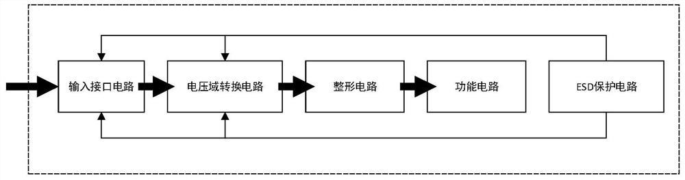
[0056] Implementation example 1: the external signal voltage domain is higher than the power supply voltage domain of the IO interface circuit, and the negative power supply of the IO interface power supply voltage domain is used as the reference ground. Assume that the power supply voltage domain of the IO interface circuit is 1.8V~0V, the external signal voltage domain is 2.4V~0.6V, and the diode conduction threshold V th is 0.4V; under this condition, the overall circuit diagram of the custom IO interface is as follows Figure 10 shown.

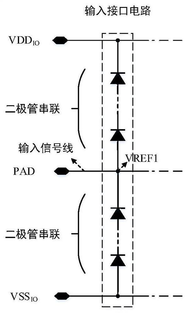
[0057] In the input interface circuit, the response range of the first reference voltage node (VREF) can be calculated by the following formula (1):

[0058]

[0059] Among them, N 1 The number of diodes that need to be inserted between the input signal line and the positive power supply network; N 2 The number of diodes that need to be inserted between the input signal line and the negative power supply network; VDD IO It is the po...

Embodiment 2

[0067] Implementation example 2: the external signal voltage domain is lower than the power supply voltage domain of the IO interface circuit, and the negative power supply of the IO interface power supply voltage domain is used as the reference ground. Assume that the power supply voltage domain of the IO interface circuit is 1.8V~0V, the external signal voltage domain is 1.2V~-0.6V, and the diode conduction threshold V th is 0.4V; under this condition, the overall circuit diagram of the custom IO interface is as follows Figure 12 shown.

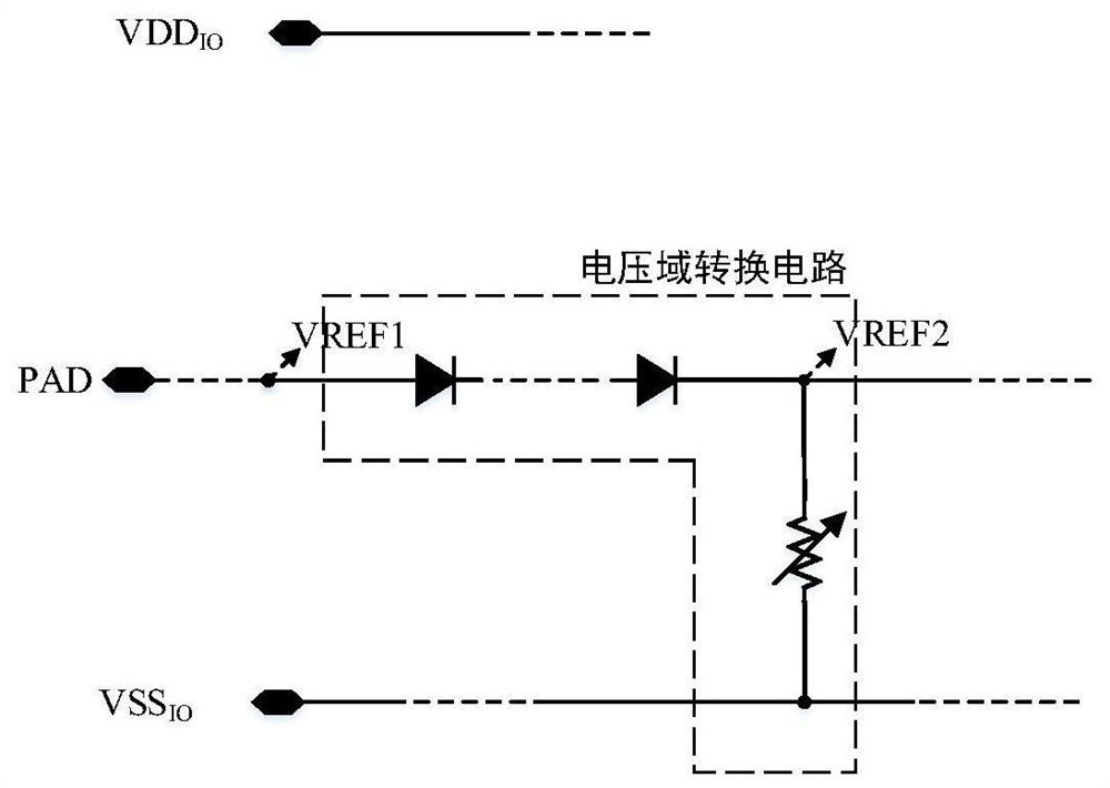
[0068] Similarly, in the input interface circuit, the response range of the first reference voltage node ( VREF1 ) can be calculated by formula (1). In order to ensure that the response range of the first reference voltage node (VREF1) matches the range of the external input signal voltage domain, it can be seen from formula (1) that at least two ESD diodes need to be inserted between the input signal line and the negative power supply ne...


PUM


Abstract

The invention belongs to the technical field of integrated circuits, and discloses a cross-power-domain circuit and a signal processing method. An input interface circuit is used for receiving an external voltage domain signal and adjusting the voltage dynamic response range of a first reference voltage node while providing a first-stage ESD discharge loop so as to match an external signal voltagedomain. The voltage domain conversion circuit is used for converting the voltage dynamic response range of the first reference point into an IO power supply voltage domain, so that a second referencevoltage node signal is subjected to correct logic judgment by an inverter in a post-stage IO power supply voltage domain. The shaping circuit comprises a first-stage shaping circuit, a second-stage shaping circuit and an ESD protection circuit, and is used for protecting potential threats formed by internal circuits. The first-stage ESD discharge loop is embedded in the input interface circuit, and meanwhile, the second-stage ESD discharge loop is embedded in the shaping circuit, so that potential threats of static electricity to an internal circuit are avoided.

Description

technical field [0001] The invention belongs to the technical field of integrated circuits, and in particular relates to a cross-power domain circuit and a signal processing method. Background technique [0002] At present, with the continuous development of integrated circuit technology, the integration of modern electronic products is getting higher and higher, and there are more and more application scenarios where chips need to communicate with external devices. When the chip communicates with external devices, in order to correctly accept the instructions issued by the external device and feed back the execution results to the external device, the chip needs to have an IO interface circuit that can correctly identify the signal of the external device and drive the external device. However, modern electronic products often contain many different subsystems or sub-circuits, such as a system on a chip (SoC). Different subsystems or subcircuits may use different devices an...

Claims


Application Information

Patent Timeline
Patent Type & Authority Applications(China)
IPC IPC(8): H03K19/0185H02H9/04
CPCH02H9/04H03K19/0185
Inventor 宋敏游龙
Owner 武汉金汤信安科技有限公司
Why Eureka
Try Eureka