Array substrate, preparation method thereof and liquid crystal display panel

A technology of array substrates and substrates, which is applied in semiconductor/solid-state device manufacturing, instruments, semiconductor devices, etc., can solve the problems of high cost, complex preparation process, high thickness of display panel, etc., achieve thickness reduction, save process technology, and reduce product cost Effect

Pending Publication Date: 2020-12-11
TCL CHINA STAR OPTOELECTRONICS TECH CO LTD
View PDF5 Cites 7 Cited by
  • Summary
  • Abstract
  • Description
  • Claims
  • Application Information

AI Technical Summary

Problems solved by technology

However, although this method can realize the function of integrated laser sensing and display, due to the complicated preparation process, the cost is high (requires more glass and process), and the thickness of the entire display panel is relatively high (glass thickness is relatively high), Unable to achieve large-scale commercial application

Method used


Image

  • Array substrate, preparation method thereof and liquid crystal display panel
  • Array substrate, preparation method thereof and liquid crystal display panel
  • Array substrate, preparation method thereof and liquid crystal display panel

Examples


Embodiment 1

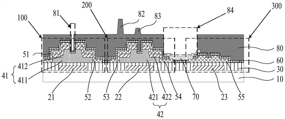
[0041] see figure 1 , a schematic structural diagram of the array substrate provided in the embodiment of the present application.

[0042] In this embodiment, the array substrate includes a substrate 10; a display thin film transistor 200, the array of display thin film transistors 200 is arranged on the substrate 10; a photosensitive thin film transistor 100, and the photosensitive thin film transistor 100 is arranged on the On the substrate 10 ; wherein, the display thin film transistor 200 and the photosensitive thin film transistor 100 are arranged in the same layer and spaced apart.

[0043] The array substrate further includes a first metal layer, a first insulating layer 30 , a semiconductor layer, a second metal layer, a second insulating layer 60 and a transparent electrode 70 stacked on the substrate 10 in sequence.

[0044] In this embodiment, the substrate 10 is a PI substrate, mainly polyimide, and the PI material can effectively improve light transmittance.

...

Embodiment 2

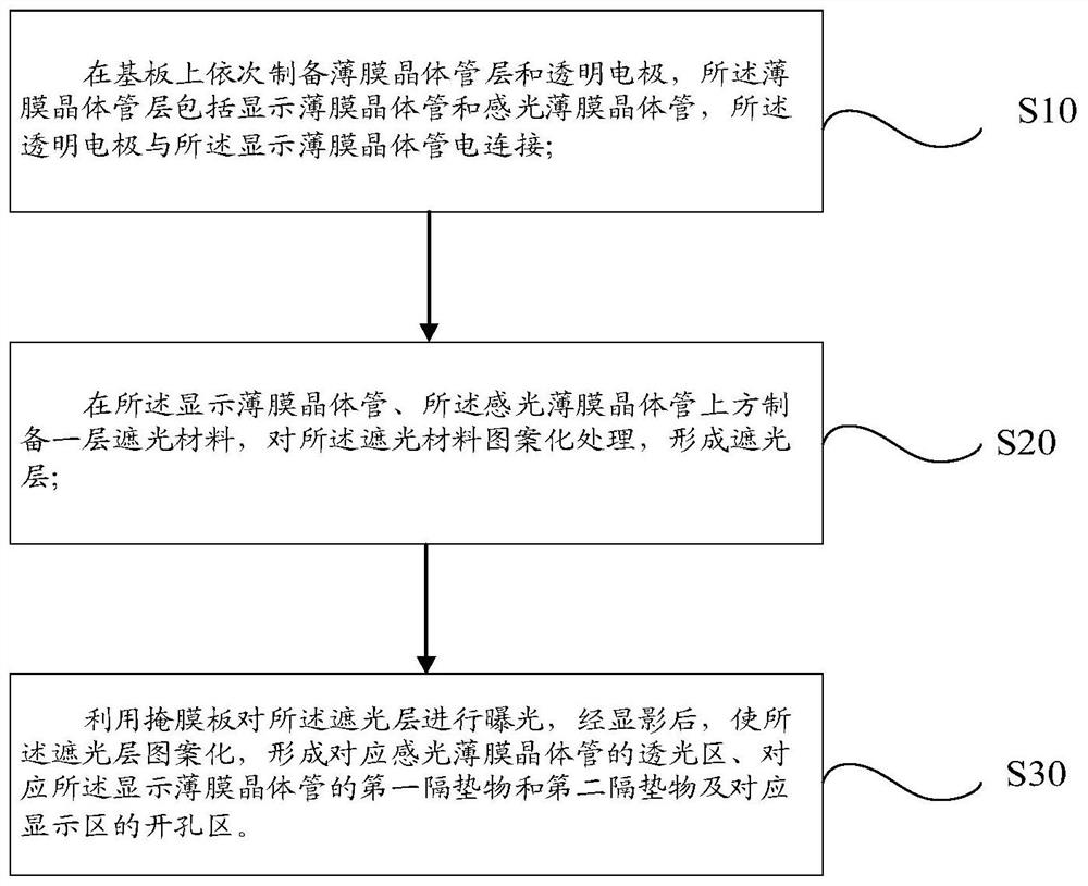
[0059] see figure 2 , a flow chart of the steps of the method for preparing the array substrate provided in the embodiment of the present application.

[0060] In this embodiment, the preparation method of the array substrate includes:

[0061] Step S10: sequentially prepare a thin film transistor layer and a transparent electrode 70 on the substrate 10, the thin film transistor layer includes a display thin film transistor 200 and a photosensitive thin film transistor 100, and the transparent electrode 70 is electrically connected to the display thin film transistor 100.

[0062] The step S10 also includes preparing a storage capacitor 300 on the substrate 10; the photosensitive thin film transistor 100, the display thin film transistor 200 and the storage capacitor 300 are arranged on the same layer and at intervals, as Figure 3A shown.

[0063] In said step S10, also include:

[0064] Step S11 : forming a first metal layer on the substrate 10 , the first metal layer in...

Embodiment 3

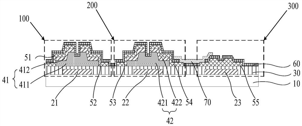
[0076] see Figure 4 , a schematic structural diagram of a liquid crystal display panel provided in an embodiment of the present application.

[0077] In this embodiment, the liquid crystal display panel includes the array substrate described in Embodiment 1, the color filter substrate 1000 and the liquid crystal layer 2000 located between the array substrate and the color filter substrate 1000 .


PUM

PropertyMeasurementUnit
transmittivityaaaaaaaaaa

Abstract

The invention provides an array substrate, a preparation method thereof and a liquid crystal display panel. The array substrate comprises: a substrate body; display thin film transistors arranged on the substrate in an array manner; and a photosensitive thin film transistor arranged on the substrate, wherein the display thin film transistor and the photosensitive thin film transistor are arrangedon the same layer at intervals. The photosensitive thin film transistor and the display thin film transistors are prepared on the same substrate, so that the functions of integrated induction and display are achieved, and meanwhile, the thickness of the array substrate can be reduced; and the light-transmitting region and other light-shielding regions of a light-shielding layer are prepared by oneprocess, so that the process technology is saved, and the product cost is reduced.

Description

technical field [0001] The present application relates to the field of display technology, in particular to an array substrate, a preparation method thereof, and a liquid crystal display panel. Background technique [0002] Thin film transistor liquid crystal display (TFT-LCD) is widely used in the current flat panel display industry because of its light, thin, small and other characteristics, low power consumption, no radiation, and relatively low manufacturing cost. In order to broaden the commercial and household functions of liquid crystal displays, many functions are now integrated into the display, such as color temperature sensing, laser sensing, gas sensing, etc., which improves the applicable scenarios of liquid crystal displays. However, many integrated functions are in the new development stage, and there are still many processes and related designs that need to be improved in order to improve the performance of various integrated function LCDs. [0003] Among th...

Claims


Application Information

Patent Timeline
Patent Type & Authority Applications(China)
IPC IPC(8): H01L27/12H01L21/77G02F1/1362
CPCH01L27/1214H01L27/1259G02F1/1362G02F1/13312G02F1/136222G02F1/136209G02F1/136213G02F1/136286G02F1/1368
Inventor 王海军
Owner TCL CHINA STAR OPTOELECTRONICS TECH CO LTD
Why Eureka
Try Eureka