Preparation method of micro LED chip

A chip and buffer layer technology, applied in semiconductor devices, electrical components, circuits, etc., can solve the problems of sidewall etching damage, reduce chip brightness, etc., and achieve the effect of reducing dislocation density, improving brightness, and reducing warpage

Active Publication Date: 2022-03-18
HCP TECH CO LTD
View PDF7 Cites 0 Cited by
  • Summary
  • Abstract
  • Description
  • Claims
  • Application Information

AI Technical Summary

Problems solved by technology

[0004] In view of the shortcomings of the prior art described above, the object of the present invention is to provide a method for preparing a Micro LED chip, which is used to solve the problem of sidewall etching damage caused by the etching process in the prior art and the source of micro LED chips. Dislocations caused by lattice mismatch and thermal stress mismatch reduce the brightness of the chip

Method used


Image

  • Preparation method of micro LED chip
  • Preparation method of micro LED chip
  • Preparation method of micro LED chip

Examples


Embodiment 1

[0036] Such as Figure 1 to Figure 4 As shown, this embodiment provides a method for preparing a Micro LED chip, and the method for preparing includes the following steps:

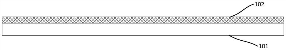
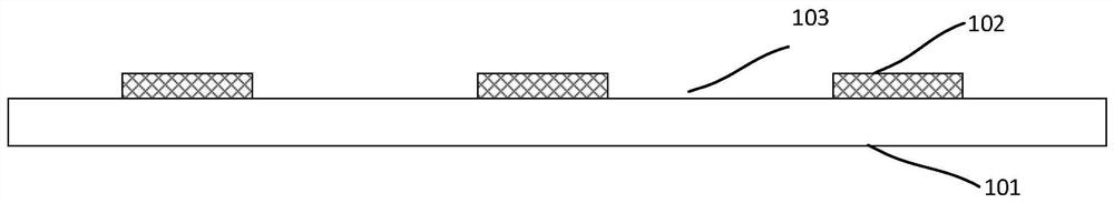
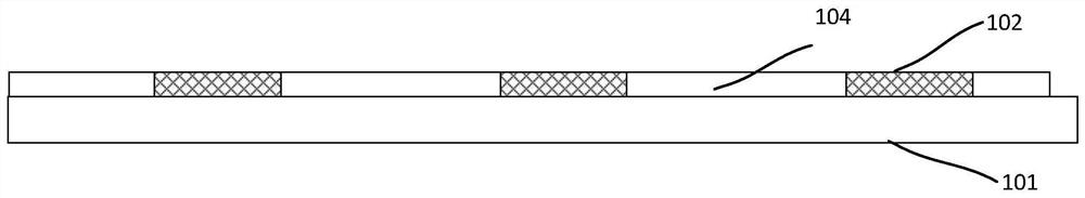
[0037] Such as Figure 1 ~ Figure 2 As shown, step 1) is first performed, a substrate 101 is provided, and a patterned buffer layer 102 is formed on the substrate 101. There is a gap 103 between adjacent buffer layers 102, and the gap 103 is covered with a mask layer. 104. However, in the prior art, the buffer layer is usually a whole.

[0038] In this embodiment, the size of the gap 103 is larger than the lateral growth size of the LED epitaxial layer in the stage of epitaxially growing the LED epitaxial layer in the subsequent step 2).

[0039] Specifically, step 1) includes the following steps:

[0040] In step 1-1), a substrate 101 is provided, and a buffer layer 102 is formed on the substrate 101 .

[0041] The substrate 101 may be a sapphire substrate or a silicon substrate, and the buffer layer ...

Embodiment 2

[0055] Such as Figure 5 As shown, this embodiment provides a method for preparing a Micro LED chip, the basic steps of which are as in Embodiment 1, wherein, the difference from Embodiment 1 is that: Step 1) also includes resetting the patterned buffer layer 102 A patterning step to improve the crystal quality of the LED epitaxial layer in step 2).

[0056] As mentioned above, the preparation method of the Micro LED chip of the present invention has the following beneficial effects:

[0057] In the present invention, during the epitaxy process of the LED epitaxial layer, no epitaxial layer is deposited on the mask layer 104, and the epitaxial layer is only deposited on the buffer layer 102, and each buffer layer 102 is a complete LED epitaxial structure, which is mutually due to The distance between the mask layers 104 makes it difficult for the LED epitaxial layers to merge laterally during the epitaxy process, thereby obtaining mutually independent LED epitaxial layers.

...


PUM


Abstract

The present invention provides a method for preparing a Micro LED chip, comprising steps: 1) providing a substrate, forming a patterned buffer layer on the substrate, with gaps between adjacent buffer layers, and the gaps are covered with a mask layer; 2) ) epitaxially grow the LED epitaxial layer on the patterned buffer layer, the LED epitaxial layer cannot be grown on the mask layer, so that there is a gap between adjacent LED epitaxial layers; 3) Micro LED chips are prepared based on the LED epitaxial layer. Through the design of the buffer layer and the mask layer, the present invention can realize an independent LED epitaxial layer on each buffer layer pattern, and can omit a process of dry etching in the traditional Micro LED process to cut out independent Micro LED chips , avoiding the sidewall etching damage caused by the etching process, and avoiding the channel of non-radiative recombination on the surface, thereby effectively improving the brightness of the Micro LED chip. The invention can also effectively reduce the warping of the LED epitaxial layer.

Description

technical field [0001] The invention belongs to the field of design and manufacture of semiconductor light emitters, in particular to a method for preparing a Micro LED chip. Background technique [0002] In the application of LED chips, the application of ordinary LED chips is mainly in lighting and display device backlight modules, and the current rapid development of Mini LED is mainly applied in indoor and outdoor display screens. However, in many applications that require higher size and PPI, the existing technology cannot meet the requirements. Therefore, Micro LED technology has emerged as a brand-new display technology. Its application concept is completely different from the previous two. It can be applied in wearable It is considered to be the ultimate display technology in the fields of wristwatches, mobile phones, car display devices, VR / AR, TVs, etc. [0003] From the perspective of technology iteration, Micro LED requires a smaller chip size to achieve a small...

Claims


Application Information

Patent Timeline
Patent Type & Authority Patents(China)
IPC IPC(8): H01L33/00H01L33/12H01L33/44
CPCH01L33/007H01L33/12H01L33/44
Inventor 庄文荣卢敬权
Owner HCP TECH CO LTD
Why Eureka
Try Eureka