A kind of semiconductor device and its preparation method

A technology for semiconductors and devices, applied in the field of semiconductor devices and their preparation, can solve problems such as poor reliability at high temperatures, and achieve the effects of increasing reliability, satisfying frequency characteristics, and expanding the scope of application

Active Publication Date: 2022-02-08
DYNAX SEMICON
View PDF4 Cites 0 Cited by
  • Summary
  • Abstract
  • Description
  • Claims
  • Application Information

AI Technical Summary

Problems solved by technology

[0005] In view of this, an embodiment of the present invention provides a semiconductor device and a manufacturing method thereof to solve the technical problem of poor high-temperature reliability of existing semiconductor devices

Method used


Image

  • A kind of semiconductor device and its preparation method
  • A kind of semiconductor device and its preparation method
  • A kind of semiconductor device and its preparation method

Examples


Embodiment Construction

[0032] In order to make the purpose, technical solution and advantages of the present invention clearer, the technical solution of the present invention will be fully described below through specific implementation in combination with the drawings in the embodiments of the present invention. Apparently, the described embodiments are some embodiments of the present invention, rather than all embodiments. Based on the embodiments of the present invention, all other embodiments obtained by persons of ordinary skill in the art without making creative efforts, All fall within the protection scope of the present invention.

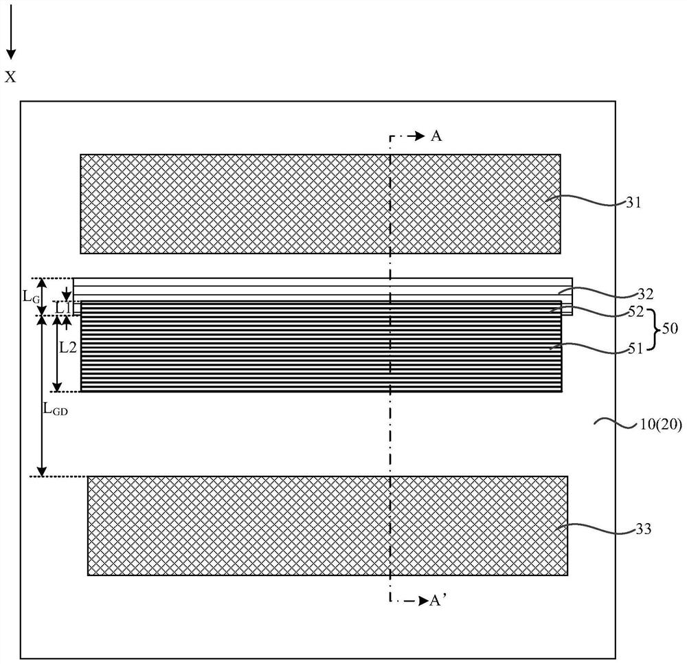
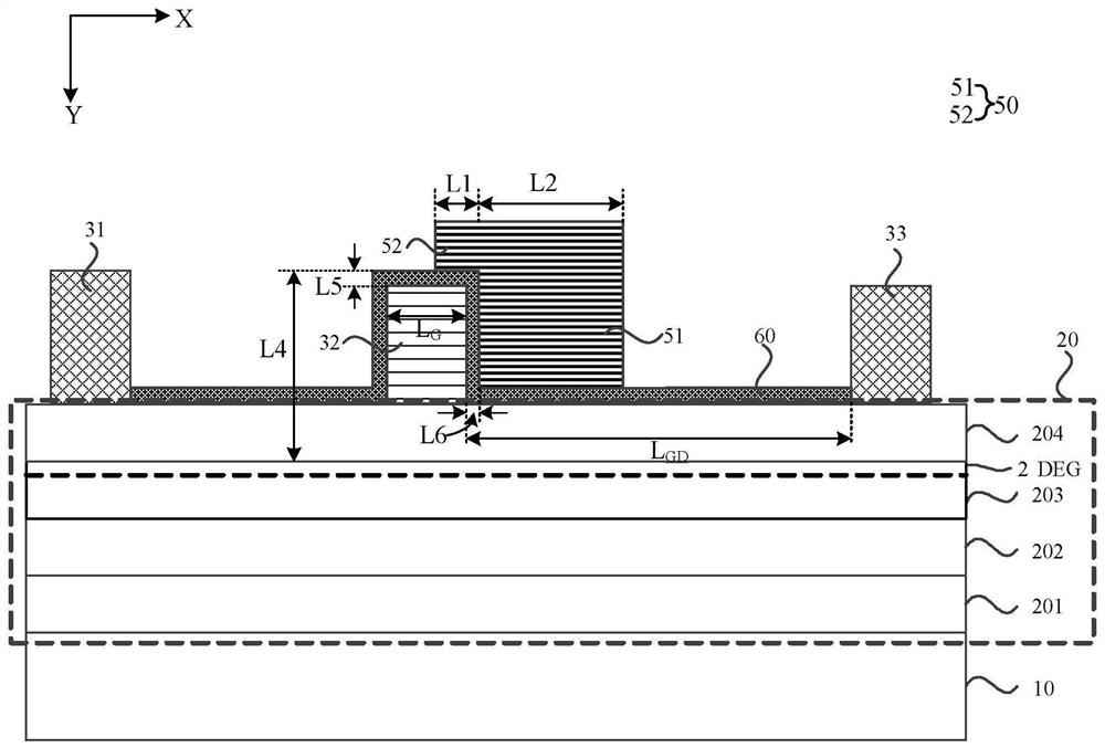
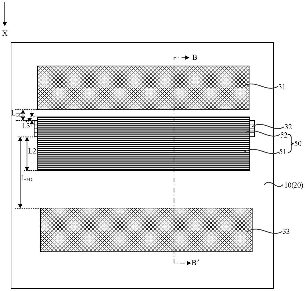
[0033] figure 1 is a schematic structural diagram of a semiconductor device provided by an embodiment of the present invention, image 3 is a schematic structural diagram of another semiconductor device provided by an embodiment of the present invention, such as figure 1 and image 3 As shown, the semiconductor device provided by the embodiment of the present...


PUM


Abstract

The embodiment of the present invention discloses a semiconductor device and a manufacturing method thereof, wherein the semiconductor device includes a substrate; a multilayer semiconductor layer located on one side of the substrate; a source electrode and a gate electrode located on the side of the multilayer semiconductor layer away from the substrate , a drain and a field plate structure, the field plate structure includes a main body and a first extension; the main body is located between the gate and the drain; the first extension is connected to the main body, and is located at the gate away from the multi-layer semiconductor layer On one side, the first extension at least partially overlaps the gate. With the above technical solution, the first extension part is set to at least partially overlap the gate, and the field plate structure is extended toward the gate side, so as to increase the modulation effect of the field plate structure on the electric field and reduce the electric field accumulation on the side of the gate close to the drain. , reduce the probability of breakdown on the side of the gate close to the drain, and at the same time set the field plate structure to extend toward the gate side, increase the facing area between the field plate structure and the gate, and increase the stability of the field plate structure, Improve the reliability of semiconductor devices.

Description

technical field [0001] Embodiments of the present invention relate to the technical field of semiconductors, and in particular to a semiconductor device and a manufacturing method thereof. Background technique [0002] Gallium nitride, a semiconductor material, has become a current research hotspot due to its characteristics of large band gap, high electron saturation drift velocity, high breakdown field strength, and good thermal conductivity. [0003] Due to the strong two-dimensional electron gas in the AlGaN / GaN heterostructure, the high electron mobility transistor (High Electron Mobility Transistor; HEMT) formed by the AlGaN / GaN heterostructure is usually a depletion device. However, in the actual working process of the device, the distribution of the electric field lines in the depletion region of the barrier layer is uneven, and most of the electric field lines are often collected at the edge of the gate close to the drain, where the electric field intensity is quite...

Claims


Application Information

Patent Timeline
Patent Type & Authority Patents(China)
IPC IPC(8): H01L29/40H01L29/778H01L21/335
CPCH01L29/402H01L29/7787H01L29/66462H01L29/7786H01L29/2003H01L29/0692H01L29/401
Inventor 裴轶刘健吴星星
Owner DYNAX SEMICON
Why Eureka
Try Eureka