Image sensor structure

An image sensor and device technology, applied in the direction of electric solid-state devices, semiconductor devices, electrical components, etc., can solve the problems of light loss, difficult structure, etc., and achieve the effect of controlling cost, improving efficiency, and improving absorption efficiency

Pending Publication Date: 2020-12-25
SHANGHAI INTEGRATED CIRCUIT RES & DEV CENT
View PDF0 Cites 2 Cited by
  • Summary
  • Abstract
  • Description
  • Claims
  • Application Information

AI Technical Summary

Problems solved by technology

The photosensitive pn junction manufactured by conventional technology generally only has a strong absorption rate and quantum efficiency for visible light, and at the same time, some light will pass through the photosensitive area and cause losses.
[00

Method used


Image

  • Image sensor structure
  • Image sensor structure
  • Image sensor structure

Examples


Example Embodiment

[0028]The specific embodiments of the present invention will be further described in detail below with reference to the accompanying drawings.

[0029]It should be noted that in the following specific embodiments, when the embodiments of the present invention are described in detail, in order to clearly show the structure of the present invention for ease of description, the structure in the drawings is not drawn according to the general scale. Partial enlargement, deformation, and simplification of processing have been implemented. Therefore, this should be avoided as a limitation of the present invention.
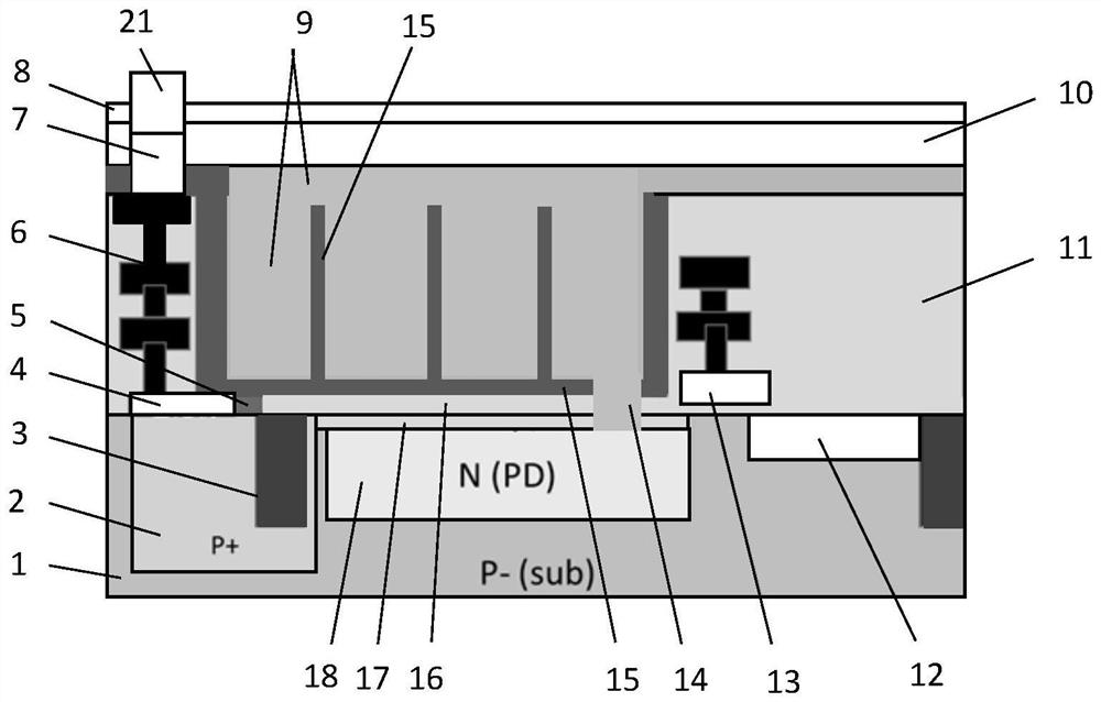
[0030]In the following specific embodiments of the present invention, please refer tofigure 1 ,figure 1 It is a schematic diagram of an image sensor structure according to a preferred embodiment 1 of the present invention. Such asfigure 1 As shown, an image sensor structure of the present invention can adopt, for example, a back-illuminated (BSI) structure, which includes a substrate...


PUM


Abstract

The invention discloses an image sensor structure. The image sensor structure comprises a substrate and a dielectric layer from bottom to top, wherein a first photosensitive device is arranged on thesubstrate, a metal interconnection layer and a second photosensitive device are arranged on the dielectric layer, the second photosensitive device is arranged in a groove, the groove is located in thedielectric layer above the first photosensitive device, and the second photosensitive device is coupled with the first photosensitive device through the groove and is led out through the metal interconnection layer, wherein the second photosensitive device comprises a plurality of pn junctions which are horizontally distributed and coupled. According to the invention, the light absorption efficiency, the full well capacity and other sensor performances can be effectively improved, and the absorption efficiency of near-infrared light can be greatly improved.

Description

technical field [0001] The invention relates to the technical field of semiconductor integrated circuits and sensors, in particular to a high-performance CMOS image sensor structure with high absorption efficiency. Background technique [0002] The photosensitive device of a traditional CMOS image sensor is usually a pn junction. The photosensitive pn junction manufactured by conventional technology generally only has a strong absorption rate and quantum efficiency for visible light, and at the same time, some light will pass through the photosensitive area and cause loss. [0003] In addition, for near-infrared light, a depletion region of several micrometers to ten micrometers or even thicker is required for effective absorption, and the implantation process of the existing CMOS process is difficult to realize this structure. Contents of the invention [0004] The object of the present invention is to overcome the above-mentioned defects in the prior art and provide an ...

Claims


Application Information

Patent Timeline
IPC IPC(8): H01L27/146
CPCH01L27/14603H01L27/1463H01L27/14636H01L27/14643
Inventor 康晓旭唐晨晨邱佳梦
Owner SHANGHAI INTEGRATED CIRCUIT RES & DEV CENT
Why Eureka
Try Eureka