A coupled resonance surface acoustic wave microfluidic chip and manufacturing method thereof

A microfluidic chip, surface acoustic wave technology, applied in chemical instruments and methods, laboratory utensils, laboratory containers, etc., can solve the problem of piezoelectric substrate fragmentation, piezoelectric substrate heating, damage to microfluidic cavity particles Or cells and other problems, to achieve the effect of improving energy efficiency

Active Publication Date: 2021-06-22
NANJING UNIV
View PDF7 Cites 0 Cited by
  • Summary
  • Abstract
  • Description
  • Claims
  • Application Information

AI Technical Summary

Problems solved by technology

However, increasing the power of the radio frequency signal will cause severe heating of the piezoelectric substrate, damage the particles or cells in the microfluidic chamber, and even cause the piezoelectric substrate to break due to overheating.

Method used


Image

  • A coupled resonance surface acoustic wave microfluidic chip and manufacturing method thereof
  • A coupled resonance surface acoustic wave microfluidic chip and manufacturing method thereof
  • A coupled resonance surface acoustic wave microfluidic chip and manufacturing method thereof

Examples


Embodiment 1

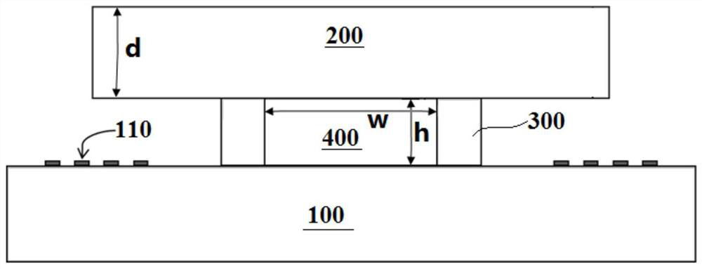
[0040] Such as figure 1 As shown, a coupled resonant surface acoustic wave microfluidic chip of the present invention includes a piezoelectric substrate 100, a cavity top cover 200 and a side wall 300, and a side wall is provided between the piezoelectric substrate 100 and the cavity top cover 200. The wall 300 , and the piezoelectric substrate 100 , the cavity top cover 200 and the side wall 300 enclose the fluid cavity 400 . It is worth noting that the longitudinal section of the piezoelectric substrate 100 of the present invention is rectangular, specifically, the piezoelectric substrate 100 is a thin plate with uniform thickness, and the piezoelectric substrate 100 is made of a flat piezoelectric material or has piezoelectric substrates attached to its surface. An ordinary solid flat plate with electrocoating, the piezoelectric substrate 100 in this embodiment is a glass plate with a zinc oxide piezoelectric thin layer grown on the surface.

[0041] It is worth further ex...

Embodiment 2

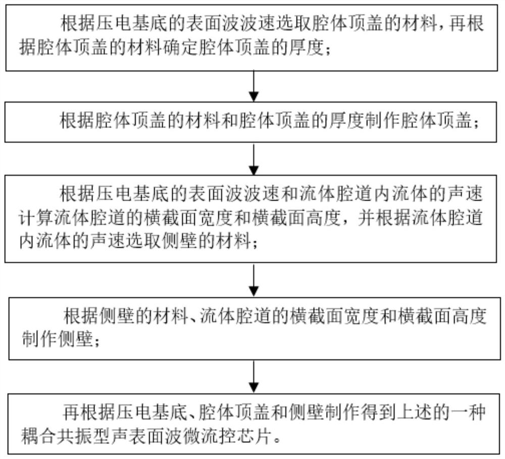
[0064] The content of this embodiment is basically the same as that of Embodiment 1. Specifically, in this embodiment, 128°Y-X lithium niobate is used as the piezoelectric substrate 100, SU-8 photoresist is used as the side wall 300, and Pyrex glass is used as the cavity top. The material of the cover 200 is water as the fluid filled in the fluid channel 400 . The specific steps of the manufacturing method of the coupled resonance surface acoustic wave microfluidic chip in this embodiment are as follows:

[0065] 1) Make cavity top cover 200

[0066] The surface wave velocity of 128°Y-X lithium niobate is c SAW =3980m / s, the present embodiment selects Pyrex glass as the cavity top cover 200 material, and its shear wave velocity is c T =3424m / s, less than c SAW =3980m / s, so it meets the requirements;

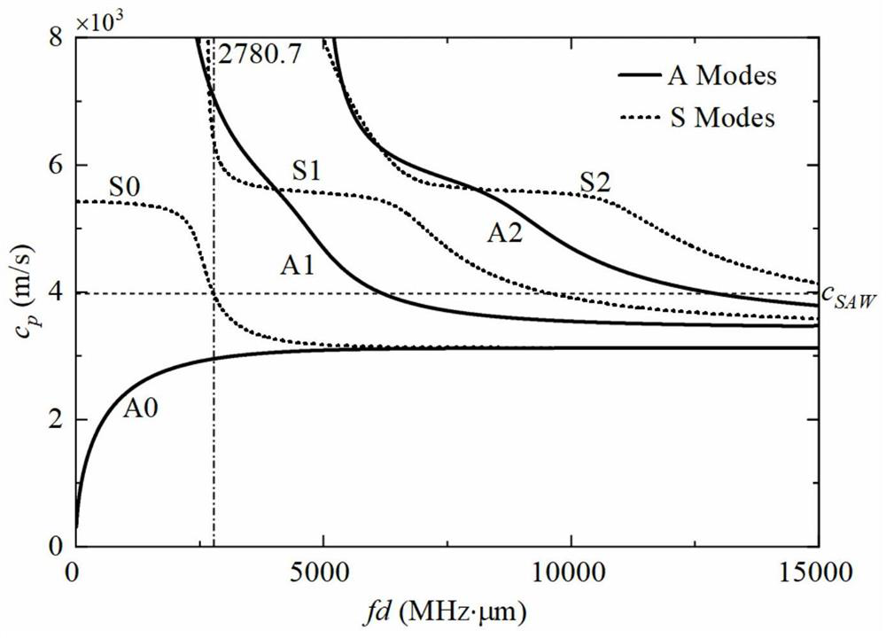
[0067] Then according to the shear wave velocity c of the Pyrex material T and longitudinal wave velocity c L =5592m / s, calculate the phase velocity dispersion curve of the...


PUM


Abstract

The invention discloses a coupled resonance surface acoustic wave microfluidic chip and a manufacturing method thereof, belonging to the technical field of microfluidic chips. The chip of the present invention includes a piezoelectric substrate, an interdigital transducer and a cavity top cover, a side wall is arranged between the piezoelectric substrate and the cavity top cover, and the piezoelectric substrate, the cavity top cover and the side wall enclose a fluid Mouth. The method of the present invention is as follows: select the material of the cavity top cover according to the piezoelectric substrate, then determine the thickness of the cavity top cover according to the working frequency and make the cavity top cover; calculate the fluid channel according to the piezoelectric substrate and the fluid in the fluid channel The cross-sectional width and cross-sectional height are selected, and the material of the side wall is selected according to the fluid in the fluid channel and the piezoelectric substrate to make the side wall; then the chip is manufactured according to the piezoelectric substrate, the cavity top cover and the side wall. The purpose of the present invention is to overcome the disadvantage of low energy of the surface acoustic wave microfluidic device in the prior art, and the present invention can improve the energy efficiency of the surface acoustic wave microfluidic chip.

Description

technical field [0001] The invention belongs to the technical field of microfluidic chips, and more specifically relates to a coupled resonant surface acoustic wave microfluidic chip and a manufacturing method thereof. Background technique [0002] Surface acoustic wave is a kind of sound wave that propagates along the solid surface, its energy is mainly concentrated in the range of 1-2 wavelengths from the surface, and the displacement amplitude decays rapidly in the depth direction. Surface acoustic wave devices use interdigital transducers on the surface of piezoelectric materials to convert radio frequency signals into surface acoustic waves, which can be used as filters, oscillators and sensors, and have many applications in medical, military, industrial, communication and other fields. In recent years, surface acoustic wave technology has been widely used in the production of acoustic microfluidic chips, which can realize functions such as particle arrangement, cell so...

Claims


Application Information

Patent Timeline
Patent Type & Authority Patents(China)
IPC IPC(8): B01L3/00
CPCB01L3/502707
Inventor 郭霞生倪正阳章东
Owner NANJING UNIV
Why Eureka
Try Eureka