Method of improving lattice damage
A lattice damage and wafer technology, applied in the field of image sensors, can solve problems such as lattice damage and affecting imaging quality
- Summary
- Abstract
- Description
- Claims
- Application Information
AI Technical Summary
Problems solved by technology
Method used
Image

Examples
Embodiment Construction
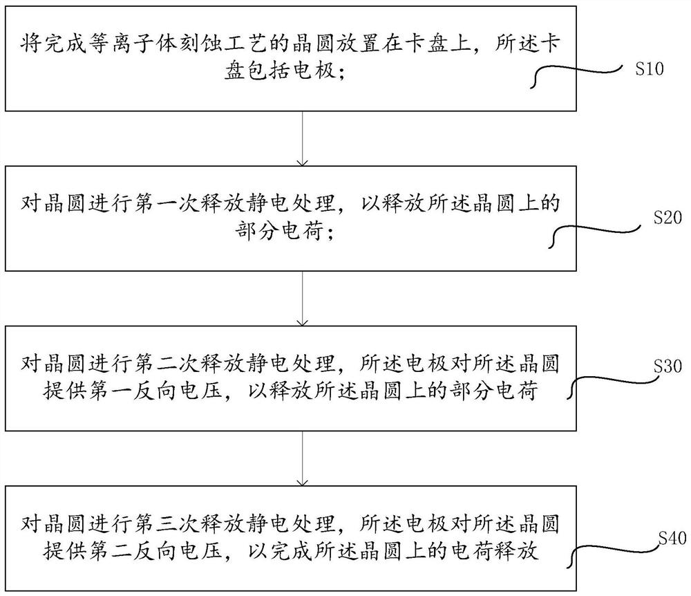
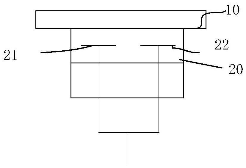
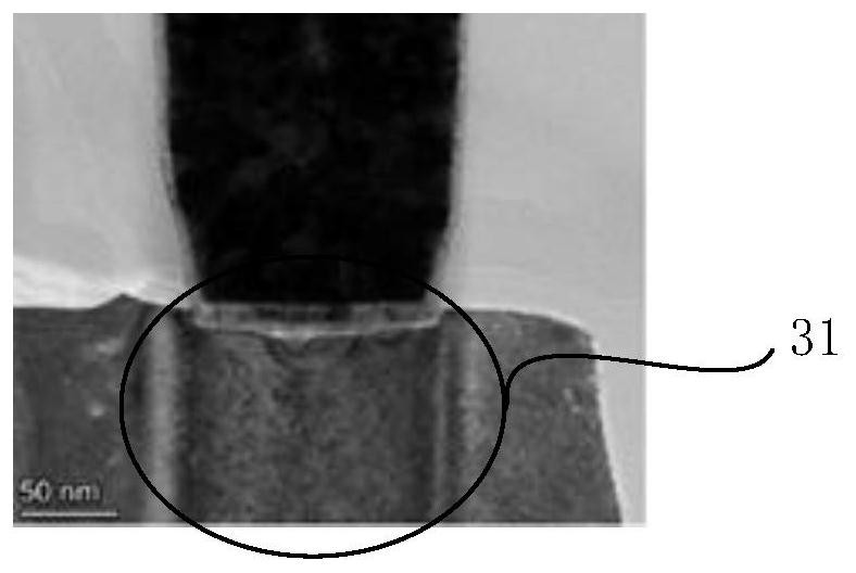
[0030] The existing sidewall etching process needs to use an etching machine to perform a sidewall etching process on the wafer to form a sidewall. During the sidewall etching process, an electrostatic adsorption chuck (ESC, Electro Static chuck) is used. Chuck) absorbs the wafer to stabilize the wafer in the reaction chamber of the etching machine for plasma etching. The electrostatic adsorption chuck adopts a double-electrode structure. In the existing process, a one-step electrostatic discharge treatment process is generally adopted. The electrostatic discharge treatment process is very fast. If the charge between the wafer and the electrostatic adsorption chuck is not completely released, the charge Gathered on the surface of the wafer, it is easy to form static electricity and damage the surface of the wafer.
[0031] A method for improving lattice damage proposed by the present invention will be described in further detail below in conjunction with the accompanying drawi...
PUM
 Abstract
Description
Claims
Application Information
 - R&D
- Intellectual Property
- Life Sciences
- Materials
- Tech Scout
- Unparalleled Data Quality
- Higher Quality Content
- 60% Fewer Hallucinations
Browse by: Latest US Patents, China's latest patents, Technical Efficacy Thesaurus, Application Domain, Technology Topic, Popular Technical Reports.
© 2025 PatSnap. All rights reserved.Legal|Privacy policy|Modern Slavery Act Transparency Statement|Sitemap|About US| Contact US: help@patsnap.com