Full-chip rapid simulation method of negative development photoetching process, negative development photoresist model, OPC model and electronic equipment

A photoresist model and photolithography process technology, applied in microlithography exposure equipment, optomechanical equipment, photolithography process exposure devices, etc., can solve the problems of low optimization speed, poor accuracy of negative development photoresist, etc. Achieve the effect of improving accuracy, improving calculation speed, and solving complex process calculations

Pending Publication Date: 2021-01-22
DONGFANG JINGYUAN ELECTRON LTD
View PDF0 Cites 1 Cited by
  • Summary
  • Abstract
  • Description
  • Claims
  • Application Information

AI Technical Summary

Problems solved by technology

[0004] In order to overcome the defects of poor simulation accuracy and low optimization speed of the negative development photoresist in the existing photolithography technology, the present invention provides a full-chip rapid simulation method for the negative development photolithography process, a negative development photoresist Models, OPC models and electronic equipment

Method used


Image

  • Full-chip rapid simulation method of negative development photoetching process, negative development photoresist model, OPC model and electronic equipment
  • Full-chip rapid simulation method of negative development photoetching process, negative development photoresist model, OPC model and electronic equipment
  • Full-chip rapid simulation method of negative development photoetching process, negative development photoresist model, OPC model and electronic equipment

Examples


Embodiment Construction

[0044] In order to make the purpose, technical solutions and advantages of the present invention more clear, the present invention will be further described in detail below in conjunction with the accompanying drawings and implementation examples. It should be understood that the specific embodiments described here are only used to explain the present invention, not to limit the present invention.

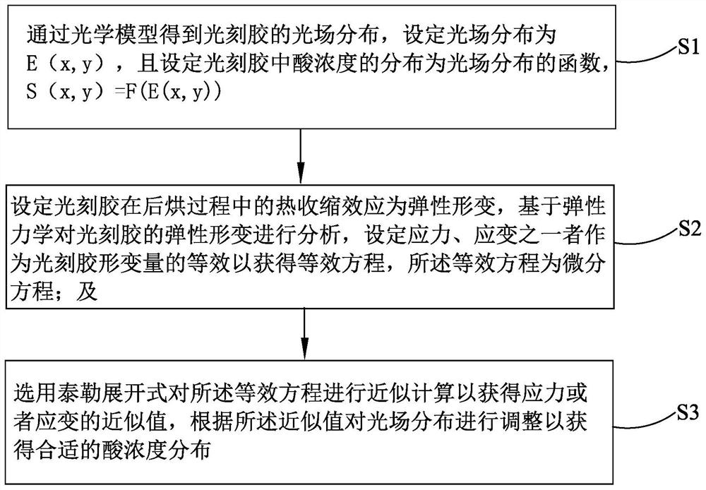
[0045] see figure 1 , the first embodiment of the present invention provides a full-chip rapid simulation method for a negative development photolithography process, including the following steps:

[0046] S1. Obtain the light field distribution of the photoresist through the optical model, set the light field distribution as E(x, y), and set the distribution of the acid concentration in the photoresist as a function of the light field distribution, that is, S(x, y)=F(E(x,y)).

[0047]In this step, the negative developing technique is an image reversal developing technique, which...


PUM

PropertyMeasurementUnit
sizeaaaaaaaaaa

Abstract

The invention relates to the technical field of integrated circuit photoetching, in particular to a full-chip rapid simulation method of a negative development photoetching process, a negative development photoresist model, an OPC model and electronic equipment. The full-chip rapid simulation method for the negative development photoetching process comprises the following steps of: analyzing the deformation of photoresist based on elastic mechanics, setting one of stress and strain as the equivalence of the deformation quantity of the photoresist to obtain an equivalent equation, and carryingout approximate calculation on the equivalent equation by selecting a Taylor expansion to obtain an approximate value of the stress or the strain; according to the approximate value, adjusting the light field distribution to obtain proper acid concentration distribution, so that the exposure pattern is closest to the target pattern, the deformation of the photoresist in the thermal shrinkage effect process can be well analyzed, the accuracy in the photoetching calculation process is improved, and meanwhile, the thermal shrinkage effect is fitted by adopting a Taylor expansion method, Therefore, the problem of complex calculation of a full-chip negative development photoetching process is solved.

Description

【Technical field】 [0001] The invention relates to the technical field of integrated circuit photolithography, and in particular to a full-chip rapid simulation method of a negative development photolithography process, a negative development photoresist model, an OPC model and electronic equipment. 【Background technique】 [0002] The photolithography process is the most important manufacturing process in the modern ultra-large-scale integrated circuit manufacturing process, that is, an important means to transfer the design pattern of the integrated circuit on the mask to the silicon wafer through the photolithography machine. As the feature size gradually shrinks, the process window available for manufacturing becomes smaller and smaller. The entire lithography process needs to be precisely controlled, and the requirements for the accuracy of computational lithography are getting higher and higher. An accurate computational lithography model can theoretically explore ways t...

Claims


Application Information

Patent Timeline
Patent Type & Authority Applications(China)
IPC IPC(8): G06F30/20G06F17/13G03F7/20G06F119/14
CPCG06F30/20G06F17/13G03F7/705G06F2119/14
Inventor 高世嘉谢理
Owner DONGFANG JINGYUAN ELECTRON LTD
Why Eureka
Try Eureka