Electro-excited photonic crystal surface-emitting laser element with photodetection structure

A technology of photonic crystals and laser components, applied in electrical components, laser components, semiconductor lasers, etc., can solve problems such as inability to integrate each other, time-consuming adjustments, and inability to integrate surface-emitting lasers and automatic power control laser modules.

Active Publication Date: 2021-09-14
PHOSERTEK CORP
View PDF1 Cites 0 Cited by
  • Summary
  • Abstract
  • Description
  • Claims
  • Application Information

AI Technical Summary

Problems solved by technology

[0002] like Figure 1A , Figure 1B As shown, a general automatic power control (Automatic Power Control, APC) laser module 40 is provided with a reflector 42 obliquely in front of a laser diode element 41. The reflector 42 can allow laser light to pass through and can reflect part of the laser light. A photodiode (Photodiode) 43 is set in the reflection path of the laser diode 43, and the photodiode 43 feeds back the optical power to the automatic power control circuit 44 that controls the laser diode element 41 to maintain the stability of the laser output power; however, due to the laser diode element 41 1. The reflector 42 and the photodiode 43 are encapsulated by a package case 45 with a lens 451 arranged at the front end. The length of the package case 45 must be increased due to the setting of the reflector 42, and the inclination of the reflector 42 is set. Corners (reflection paths) may require lengthy adjustments
[0003] figure 2 As shown, it discloses China Taiwan Patent No. I303505, which is a surface-emitting laser 50, comprising: an n-doped gallium arsenide (GaAs) substrate 51, an n-doped first mirror The structure 52 is formed on the GaAs substrate 51; the lower cladding layer 53 is deposited on the first mirror structure 52; an active layer 54 is formed on the lower cladding layer 53; an upper cladding layer 55 is formed on the active layer 54; A second mirror structure 56 is formed on the upper cladding layer 55, a p-type electrode 57 is formed on the second mirror structure 56, and an n-type electrode 58 is formed on the bottom surface of the substrate 51; however, the surface-emitting laser 50 The laser is emitted directly, and the power ratio of the laser cannot be automatically controlled
[0004] Since the automatic power control laser module and the surface-emitting laser cannot be integrated with each other
Therefore, in view of the problems disclosed above, the inventor of this case conceived to use photonic crystal (Photonic crystal, PC) to solve the problem that the surface-emitting laser and the automatic power control laser module cannot be integrated with each other, which is the problem to be solved by the present invention

Method used


Image

  • Electro-excited photonic crystal surface-emitting laser element with photodetection structure
  • Electro-excited photonic crystal surface-emitting laser element with photodetection structure
  • Electro-excited photonic crystal surface-emitting laser element with photodetection structure

Examples


Embodiment Construction

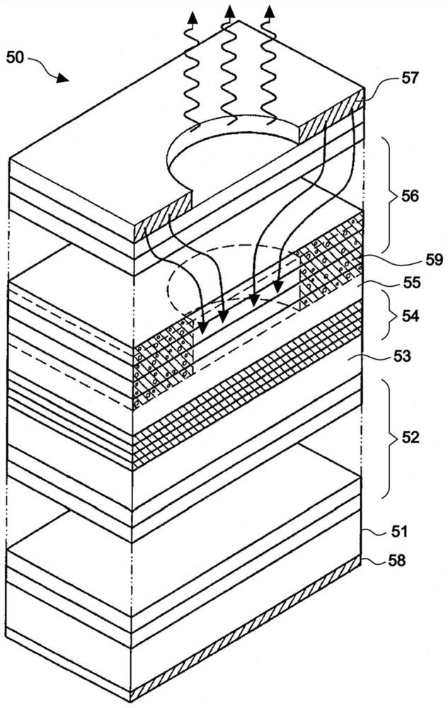
[0049] First, see Figure 3A ~ Figure 3M As shown, the present invention provides a preferred embodiment of an electrically excited photonic crystal surface-emitting laser element (Electrically Pumped Photonic-Crystal Surface-Emitting Lasers) 10A with a photodetection structure, which extends the applicant's use of electrically excited photonic crystal surface Application number 16 / 008,223 filed by the U.S. Patent and Trademark Office, and the electro-excited photonic crystal surface-emitting laser element has been notified for approval and has not yet been published and announced, including: a substrate (substrate) 11, which has A first surface 111 and a second surface 112 on the opposite side. In this embodiment, the material of the substrate 11 can be selected from any of gallium nitride (GaN), gallium arsenide (GaAs), and indium phosphide (InP) formed, but not limited to.

[0050] A cladding layer (Cladding layer) 12 is located on the first surface 111 of the substrate 11...


PUM

PropertyMeasurementUnit
thicknessaaaaaaaaaa
thicknessaaaaaaaaaa
thicknessaaaaaaaaaa

Abstract

An electro-excited photonic crystal surface-emitting laser element with a photodetection structure, including: a plurality of air holes, each air hole forms a photonic crystal structure with a primary structure and a secondary structure by changing the size ratio and position of the air holes, and the After the light introduction ratio of the light introduction channel of the secondary structure reaches the photodetection structure, a readable photodetection signal is formed, and the strength of the photodetection signal can be used to know the power ratio of the laser emitted by the surface of the photonic crystal structure, so the automatic The power control circuit utilizes the intensity of the photodetection signal of the photodetection structure to feed back and control the power ratio of the laser beam emitted from the surface of the photonic crystal structure, thereby having automatic power control of the surface-emitting laser.

Description

technical field [0001] The present invention relates to an electro-excited photonic crystal surface-emitting laser element with a photonic crystal structure. The light-introduction channel is made in the photonic crystal structure to the light-introduction structure, and the light-introduction of the laser in the light-introduction channel can be detected by the photodetection structure. The ratio can also be used to know the power ratio of the emitted laser light on the surface of the photonic crystal structure. Background technique [0002] Such as Figure 1A , Figure 1B As shown, a general automatic power control (Automatic Power Control, APC) laser module 40 is provided with a reflector 42 obliquely in front of a laser diode element 41. The reflector 42 can allow laser light to pass through and can reflect part of the laser light. A photodiode (Photodiode) 43 is set in the reflection path of the laser diode 43, and the photodiode 43 feeds back the optical power to the ...

Claims


Application Information

Patent Timeline
Patent Type & Authority Patents(China)
IPC IPC(8): H01S5/183H01S5/20H01S5/02257
CPCH01S5/18H01S5/20H01S5/0264H01S5/18319H01S5/18327H01S5/34333H01S5/04253H01S5/11H01S5/026H01S5/18308H01S5/3216
Inventor 林国瑞陈俞谌
Owner PHOSERTEK CORP
Why Eureka
Try Eureka