Supercharge Your Innovation With Domain-Expert AI Agents!

Drilling method of large-size printed board

A drilling method and technology for printed boards, which are applied in the directions of printed circuit manufacturing, printed circuits, and circuit board tool positioning, can solve the problems of printed circuit board drilling and hole deviation, achieve good alignment and reduce production costs. , Improve the effect of drilling quality

Active Publication Date: 2021-01-22
JIANGMEN SUNTAK CIRCUIT TECH
View PDF5 Cites 2 Cited by
  • Summary
  • Abstract
  • Description
  • Claims
  • Application Information

AI Technical Summary

Problems solved by technology

[0004] The present invention aims at the problem of the above-mentioned defects in the existing circuit board, and provides a method for drilling large-sized printed circuit boards, which can solve the problems of drilling and hole deviation of printed circuit boards whose size exceeds the size of the drilling machine

Method used


Image

  • Drilling method of large-size printed board

Examples


Embodiment

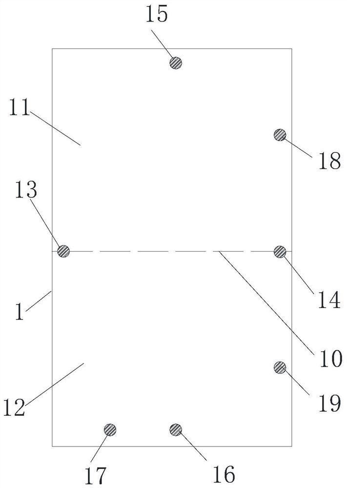
[0031] A method for manufacturing a printed board shown in this embodiment includes a drilling method for a large-sized printed board, and includes the following processing steps in turn:

[0032] (1) Cutting: cut out the core board according to the panel size 520mm×820mm, the thickness of the core board is 1mm, and the thickness of the outer copper surface of the core board is 1OZ; and the core board 1 is divided by the center line of the long side 10 Divided into first half 11 and second half 12 (such as figure 1 shown).

[0033] (2), making the inner layer circuit (negative film process): according to the pattern positioning hole, use a vertical coating machine to coat the photosensitive film on the core plate. grid exposure ruler (21 grid exposure rulers) to complete the exposure of the inner layer circuit and the inner layer target, and form the inner layer circuit pattern and target pattern after development; the inner layer etching, etch the inner layer circuit and mul...


PUM


Abstract

The invention discloses a drilling method for a large-size printed board, and the method comprises the following steps: manufacturing an inner-layer circuit and targets on a core board, wherein the targets comprise a first target, a second target, a third target and a fourth target which are located in the middle of four board edges, a fifth target disposed on a short edge, and a sixth target anda seventh target which are disposed on a long edge; pressing the core plate and the outer-layer copper foil into a production plate through prepregs; drilling a target hole in the position corresponding to the target through an XRAY target-shooting machine; measuring the target distance between the target holes in the long side and the short side, comparing the target distance with a target distance standard value, and calculating the drilling belt coefficient needed during drilling; taking the first target hole, the second target hole and the third target hole as positioning points, and performing drilling machining on the front half portion of the production plate according to the drilling belt coefficient; taking the first target hole, the second target hole and the fourth target hole as positioning points, and performing drilling machining on the rear half portion of the production plate according to the drilling belt coefficient. The method can solve the problems of drilling and hole deviation of the printed circuit board of which the size exceeds the machining size of a drilling machine.

Description

technical field [0001] The invention relates to the technical field of printed circuit board production, in particular to a method for drilling large-sized printed circuit boards. Background technique [0002] In the production of printed circuit boards, in order to improve the utilization rate of boards, reduce production costs, and increase per capita efficiency and output value, the imposition production method is adopted. According to the product design size, the large material is first produced in the production unit PNL, and the PNL is divided into several Delivery units SET, each SET is then composed of a certain number of product units PCS. [0003] The production process of printed circuit boards is: cutting material→making inner layer circuit→pressing→drilling→sinking copper→full board electroplating→making outer layer circuit→making solder mask→surface treatment→forming→FQC; In the drilling process, due to the limitation of the maximum size of the product that ca...

Claims


Application Information

Patent Timeline
IPC IPC(8): H05K3/00B26F1/16
CPCH05K3/0047H05K3/0008B26F1/16H05K2203/0221B26F2210/08
Inventor 张细海寻瑞平刘红刚戴勇
Owner JIANGMEN SUNTAK CIRCUIT TECH
Features
  • R&D
  • Intellectual Property
  • Life Sciences
  • Materials
  • Tech Scout
  • Unparalleled Data Quality
  • Higher Quality Content
  • 60% Fewer Hallucinations
Learn More