

Silicon wafer roughening solution
A technology of silicon wafer and hair liquid, which is applied in the field of electronic chemicals, can solve problems such as tip discharge and affect the performance of IGBT devices, and achieve the effects of improving oxidation, eliminating sharp corners on microscopic surfaces, and reducing the activation energy of initial reactions
- Summary
- Abstract
- Description
- Claims
- Application Information
AI Technical Summary
Problems solved by technology
Method used
Image

Examples
Embodiment 1-14
[0063] The content of each component according to the conceived examples and comparative examples of the present invention is listed in Table 1, and the balance is water.
[0064] Table 1
[0065]
[0066]
[0067] The above-mentioned embodiments 1-14 are all configured according to the following steps:
[0068] (1) Sampling according to the ratio in the above table for later use;
[0069] (2) Slowly add mineral acid to the oxidizing agent, mix well, and cool to below 40°C;
[0070] (3) Add fluorine-containing compound in the mixed acid of step (2), mix evenly, set aside;
[0071] (4) Add the long-chain organic matter into the buffer and mix evenly, and then slowly add the mixed solution into the mixed acid in step (2), mix evenly, and obtain the hair removal solution described in Examples 1-6.
[0072] The above comparative example 1 is configured according to the following steps:
[0073] (1) according to mass percent sulfuric acid 70%, nitric acid 6% and hydrofluo...
PUM
| Property | Measurement | Unit |
|---|---|---|
| electrical resistivity | aaaaa | aaaaa |
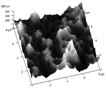
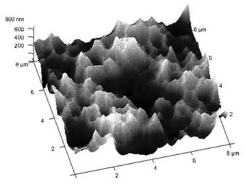
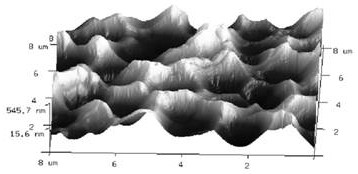
| surface roughness | aaaaa | aaaaa |
Abstract
Description
Claims
Application Information