

Epitaxial substrate embedded with metal-based nitride material and preparation method thereof
An epitaxial substrate and nitrogen-based technology, which is applied in semiconductor/solid-state device manufacturing, electrical components, electrical solid-state devices, etc., can solve the problems of poor heat dissipation of third-generation nitride materials and devices, and achieve the goal of improving reliability and performance Effect
- Summary
- Abstract
- Description
- Claims
- Application Information
AI Technical Summary
Problems solved by technology
Method used
Image

Examples
preparation example Construction
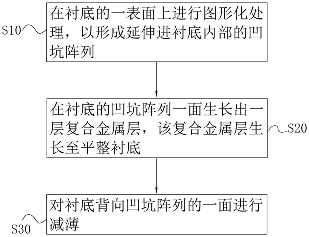
[0033] see figure 2 As shown, the present invention relates to a method for preparing an epitaxial substrate with an embedded metal-based nitride material, comprising the following steps:
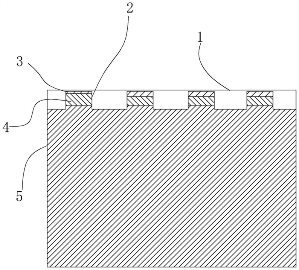
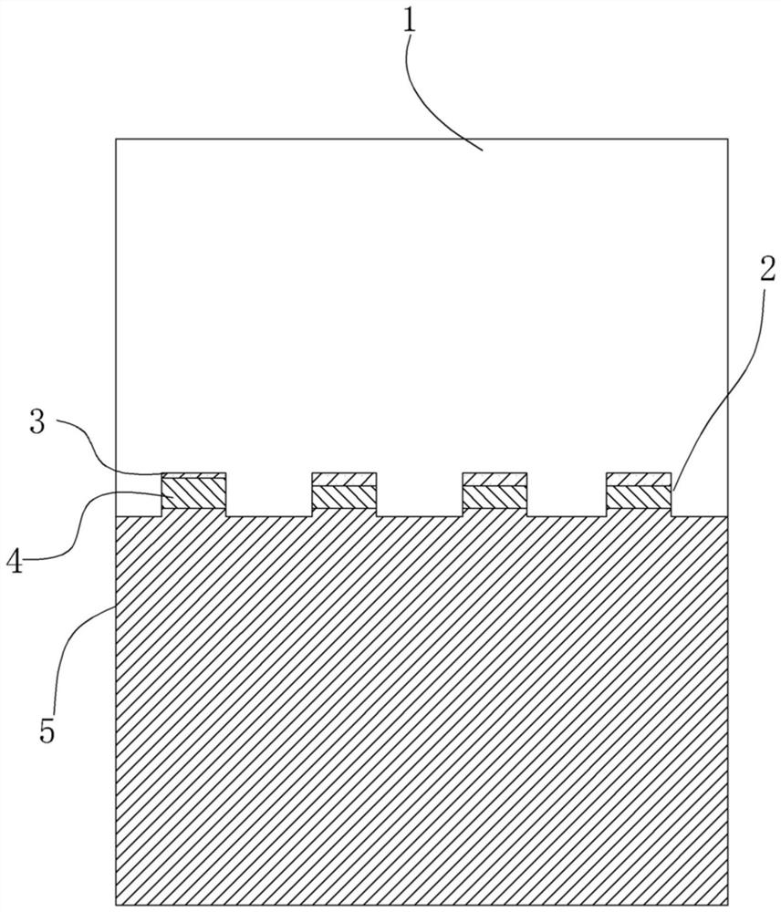
[0034] S10. Perform patterning on a surface of the substrate to form an array of pits extending into the interior of the substrate;
[0035] S20, growing a layer of composite metal layer on the pit array side of the substrate, and the composite metal layer is grown to cover the substrate;
[0036] S30. Thinning the side of the substrate facing away from the pit array.
[0037] Firstly, the present invention performs patterning on the substrate, increases the contact area between the subsequent composite metal layer and the substrate, and is closer to the functional layer of the epitaxial material device, so as to maximize the heat conduction path, and secondly, it can well release the metal medium and the traditional material The thermal mismatch and lattice mismatch stress, the size of ...
no. 1 example
[0052] The substrate selected in this embodiment is a 2-inch aluminum nitride substrate with a thickness of 430 μm, a crystal orientation of 001, and a resistivity greater than 107 Ω.cm. The aluminum nitride substrate is uniformly glued and developed through a semiconductor process. and etching to form a pit array with a depth of 5 μm on the surface; then use PVD to deposit a layer of 0.1 μm first copper layer on the pit array; Copper layer, the second copper layer fills the pit array; finally, the third copper layer is electroplated by electroplating, and the thickness of the third copper layer is thickened to 150 μm; finally, the aluminum nitride substrate faces the pit One side of the pit array was first thinned to 300 μm, and then annealed in a medium-temperature bottom annealing furnace for 5 hours under 600-degree nitrogen gas; then the second thinning was performed to 150 μm, and then The annealing time is 3 hours under the condition of 600 degrees nitrogen in the high ...
no. 2 example
[0055] The substrate selected in this embodiment is a 2-inch aluminum nitride substrate with a thickness of 430 μm, a crystal orientation of 001, and a resistivity greater than 107 Ω.cm. The aluminum nitride substrate is uniformly glued and developed through a semiconductor process. and etching to form a pit array with a depth of 5 μm on the surface; then use PVD to deposit a layer of 0.1 μm first copper layer on the pit array; Copper layer, the second copper layer fills the pit array; finally, the third copper layer is electroplated by electroplating, and the thickness of the third copper layer is thickened to 150 μm; finally, the aluminum nitride substrate faces the pit One side of the pit array was first thinned to 300 μm, and then annealed in a medium-temperature bottom annealing furnace for 5 hours under 600-degree nitrogen gas; then the second thinning was performed to 150 μm, and then The annealing time is 3 hours under the condition of 600 degrees nitrogen in the high ...
PUM
| Property | Measurement | Unit |
|---|---|---|
| Thickness | aaaaa | aaaaa |
| Thickness | aaaaa | aaaaa |
| Thickness | aaaaa | aaaaa |
Abstract
Description
Claims
Application Information