Check patentability & draft patents in minutes with Patsnap Eureka AI!

Semiconductor process equipment

A process equipment and semiconductor technology, applied in discharge tubes, electrical components, circuits, etc., can solve problems such as low efficiency, long maintenance time, and poor adjustment accuracy.

Pending Publication Date: 2021-02-05
BEIJING NAURA MICROELECTRONICS EQUIP CO LTD
View PDF0 Cites 0 Cited by
  • Summary
  • Abstract
  • Description
  • Claims
  • Application Information

AI Technical Summary

Problems solved by technology

However, the way to adjust the inductive coupling power and capacitive coupling power in the prior art is usually to manually adjust the position of components such as the ICP coil in the equipment and the relative distance between the components by the operator, the adjustment accuracy is poor and the maintenance time is long ,low efficiency

Method used


Image

  • Semiconductor process equipment
  • Semiconductor process equipment
  • Semiconductor process equipment

Examples


Embodiment Construction

[0024] Specific embodiments of the present invention will be described in detail below in conjunction with the accompanying drawings. It should be understood that the specific embodiments described here are only used to illustrate and explain the present invention, and are not intended to limit the present invention.

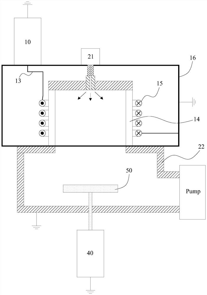
[0025] like figure 1 Shown is a schematic structural view of a semiconductor process equipment in the prior art, which includes a radio frequency power supply 10, a dielectric cylinder 14, a gas supply assembly 21, a shielding box 16, a reaction chamber 22, a lower electrode power supply 40, a lower electrode 50, and a The connecting wire 13 is electrically connected to the ICP coil 15 of the radio frequency power supply 10 . Among them, the gas supply component 21 is used to supply the process gas into the medium cylinder 14, and the ICP coil 15 receives the radio frequency signal of the radio frequency power supply 10 through the connection line 13 and excite...


PUM

PropertyMeasurementUnit
Frequencyaaaaaaaaaa

Abstract

The invention provides semiconductor process equipment, which comprises an excitation coil, a process chamber, a radio frequency source assembly and an adjusting assembly, and is characterized in thatthe radio frequency source assembly is electrically connected with the excitation coil and is used for providing radio frequency power for the excitation coil, and the excitation coil is arranged around the process chamber; and the first end of the adjusting assembly is electrically connected with the end, connected with the radio frequency source assembly, of the excitation coil, the second endof the adjusting assembly is grounded, and the adjusting assembly is used for adjusting load impedance of the radio frequency source assembly. According to the semiconductor process equipment providedby the invention, the exciting coil and the adjusting assembly are arranged in parallel, and the adjusting assembly can flexibly and efficiently change the power distribution relationship between theinductive coupling parallel branch and the capacitive coupling parallel branch and the input voltage of the input end of the exciting coil, so that the precise control on the plasma density and components is realized.

Description

technical field [0001] The present invention relates to the field of semiconductor equipment, in particular, to a semiconductor process equipment. Background technique [0002] Plasma processing equipment is widely used in the semiconductor industry, and inductively coupled plasma (ICP) equipment is one of the most widely used plasma generating devices. The ICP source generates plasma by means of radio-frequency coupling discharge, and then processes such as etching and deposition through the plasma. [0003] Existing ICP plasma devices usually include a radio frequency power supply and an ICP coil electrically connected to the radio frequency power supply. After the radio frequency signal of the radio frequency power supply reaches the ICP coil, the high frequency electromagnetic field generated by the coil excites the process gas passing into the process chamber to generate plasma . Among them, the power coupled from the ICP coil to the plasma usually includes two parts:...

Claims


Application Information

Patent Timeline
IPC IPC(8): H01J37/32
CPCH01J37/321H01J37/32183
Inventor 李兴存
Owner BEIJING NAURA MICROELECTRONICS EQUIP CO LTD
Features
  • R&D
  • Intellectual Property
  • Life Sciences
  • Materials
  • Tech Scout
  • Unparalleled Data Quality
  • Higher Quality Content
  • 60% Fewer Hallucinations
Learn More