Preparation method of semiconductor structure

A semiconductor and reactive gas technology, applied in semiconductor/solid-state device manufacturing, electrical components, circuits, etc., can solve the problems of excessive grinding time, different grinding rates, active area damage, etc., to reduce the amount of grinding and improve the surface Uniformity, the effect of reducing the damage of the active area

Active Publication Date: 2021-02-05
SHANGHAI HUAHONG GRACE SEMICON MFG CORP +1
View PDF6 Cites 0 Cited by
  • Summary
  • Abstract
  • Description
  • Claims
  • Application Information

AI Technical Summary

Problems solved by technology

However, in the chemical mechanical polishing process of isolation trenches, too long polishing time or overpolishing time may cause excessive polishing, resulting in serious active area damage (AA damage, ie figure 1 the situation indicated)
At the same time, due to the high selectivity of the polishing liquid, the isolation trench and the hard mask layer have different polishing rates. When the chemical mechanical polishing process stays on the hard mask layer, the isolation trench Scratches may form on the surface (Micro scratch, ie figure 2 The situation represented) and dishing (disshing), thus affecting the uniformity of the wafer (Within Wafer, WIW)

Method used


Image

  • Preparation method of semiconductor structure
  • Preparation method of semiconductor structure
  • Preparation method of semiconductor structure

Examples


preparation example Construction

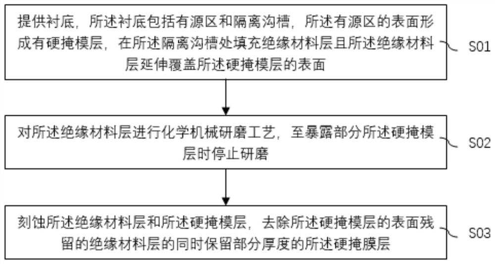
[0027] image 3 For a preparation method of a semiconductor structure provided by an embodiment of the present invention, refer to image 3 It can be seen that the method for preparing the semiconductor structure provided in this embodiment includes:

[0028] Step S01: providing a substrate, the substrate includes an active region and an isolation trench, a hard mask layer is formed on the surface of the active region, an insulating material layer is filled at the isolation trench, and the insulating material a layer extending over a surface of the hard mask layer;

[0029] Step S02: performing a chemical mechanical polishing process on the insulating material layer, and stopping polishing when a part of the hard mask layer is exposed;

[0030] Step S03: Etching the insulating material layer and the hard mask layer, removing the remaining insulating material layer on the surface of the hard mask layer while retaining a partial thickness of the hard mask layer.


PUM


Abstract

The invention provides a preparation method of a semiconductor structure, which comprises the following steps: providing a substrate which comprises an active region and an isolation trench, forming ahard mask layer on the surface of the active region, filling an insulating material layer at the isolation trench, and extending the insulating material layer to cover the surface of the hard mask layer; performing a chemical mechanical polishing process on the insulating material layer, and stopping polishing until a part of the hard mask layer is exposed; and etching the insulating material layer and the hard mask layer, removing the residual insulating material layer on the surface of the hard mask layer, and retaining part of the thickness of the hard mask layer. According to the preparation method of the semiconductor structure provided by the invention, the grinding amount is reduced by monitoring the grinding end point of the chemical mechanical grinding process in real time and setting the over-grinding time to be zero, so that active region damage caused by over-grinding is reduced, the surface uniformity of the semiconductor structure is improved, and scratches and dish-shaped recesses are avoided.

Description

technical field [0001] The invention relates to the technical field of semiconductors, in particular to a method for preparing a semiconductor structure. Background technique [0002] In the semiconductor manufacturing process, the isolation trench (Shallow Trench Isolation, STI) has the advantages of good isolation effect and small occupied area. A typical isolation trench (STI) preparation process includes: oxide layer deposition process, hard mask layer deposition process, isolation trench etching process, isolation trench filling process, chemical mechanical polishing (CMP) , a hard mask layer removal process and an oxide layer removal process. [0003] Wherein, during the chemical mechanical polishing process (i.e. STI-CMP process) of the isolation trench, the purpose of performing chemical mechanical polishing is to remove the redundant filler in the isolation trench filling process and make the surface of the isolation trench smooth. In order to achieve the above p...

Claims


Application Information

Patent Timeline
Patent Type & Authority Applications(China)
IPC IPC(8): H01L21/762H01L21/3105H01L21/311
CPCH01L21/76224H01L21/31053H01L21/31116Y02P70/50
Inventor 许秀秀梁金娥
Owner SHANGHAI HUAHONG GRACE SEMICON MFG CORP
Why Eureka
Try Eureka