

Semiconductor element reliability evaluation device and semiconductor element reliability evaluation method
A technology for evaluating devices and semiconductors, which can be used in single semiconductor device testing, semiconductor working life testing, measuring devices, etc., and can solve problems such as semiconductor component damage
- Summary
- Abstract
- Description
- Claims
- Application Information
AI Technical Summary
Problems solved by technology
Method used
Image

Examples
Embodiment approach 1
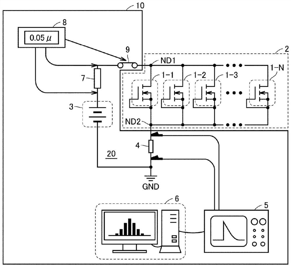
[0033] figure 1 It is a block diagram of the reliability evaluation apparatus of the semiconductor element of Embodiment 1.
[0034] The semiconductor elements 1 - 1 to 1 -N to be tested are MOSFETs, IGBTs, or the like. The semiconductor elements 1 - 1 to 1 -N are not limited to self-arc-extinguishing elements, and may be rectifying elements such as PiN diodes or Schottky barrier diodes. The material of the semiconductor element is not limited to general Si, and may be SiC, GaN, Ga203, diamond, etc. with a large band gap.
[0035] exist figure 1 In , N self-arcing type semiconductor elements 1 - 1 to 1 -N are shown. The semiconductor element 1-1 is referred to as a first test object semiconductor element, and the semiconductor element 1-N is referred to as an Nth test object semiconductor element. The test circuit 2 is configured by connecting the semiconductor elements 1 - 1 to 1 -N in parallel. The same voltage is applied to the semiconductor elements 1-1 to 1-N. The r...
Embodiment approach 2
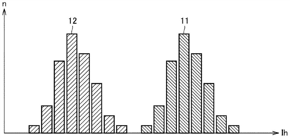
[0062] In Embodiment 2, the analyzer 6 performs analysis processing on the analysis item B. FIG. Analysis item B is the duration of the pulse. The duration of the pulse corresponds to the temporal width of the pulse. The duration of the pulse can be set to the time from when the leakage current exceeds the determined threshold to when the leakage current falls to the determined threshold.
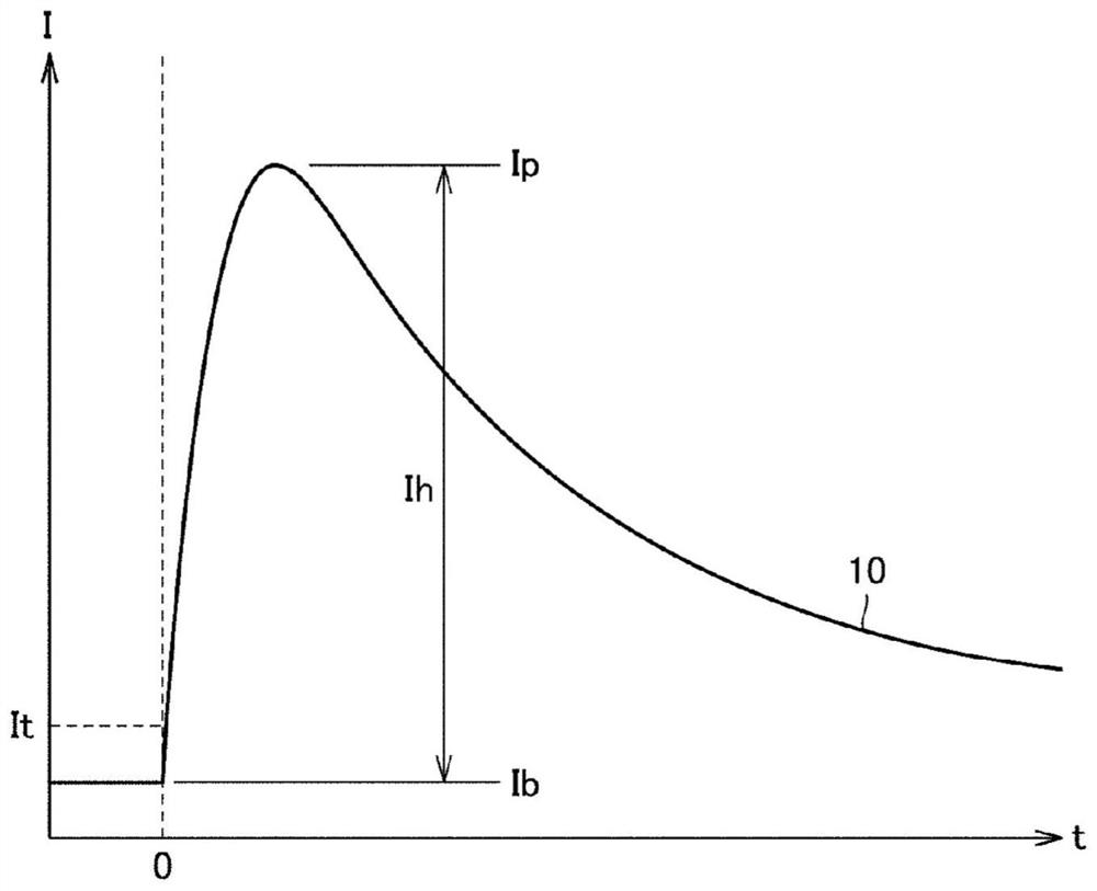
[0063] Figure 4 It is a figure for explaining analysis item B. exist Figure 4 The pulse waveform 40 of the leakage current measured by the measuring device 5 is shown as an example in . exist Figure 4 Among them, the horizontal axis represents the time t, and the vertical axis represents the magnitude of the leakage current I.
[0064] At time 0 on the time axis, the leakage current I exceeds the first threshold It0. As a result, the measuring device 5 records the waveform. It0 may be the same value as It in the first embodiment. The leakage current changes in a pulse shape. Th...
Embodiment approach 3
[0072] In Embodiment 3, the analyzer 6 performs analysis processing on the analysis item C. Analysis item C is the frequency of pulse generation. The pulse generation frequency can be set to the number of pulses in which the leakage current I exceeds the determined threshold value generated per unit time.
[0073] Figure 6 It is a figure for explaining analysis item C. exist Figure 6 The pulse waveform 40 of the leakage current measured by the measuring device 5 is shown as an example in . The horizontal axis represents time t, and the vertical axis represents leakage current I. At time 0 on the time axis, the leakage current I exceeds the threshold It. As a result, the measuring device 5 records the waveform. The analyzer 6 calculates the generation frequency of pulses per unit time based on the number of recorded waveforms. Even if the leakage current I fluctuates instantaneously, in such as Figure 6 When the leakage current I does not exceed the threshold value I...
PUM
 Abstract
Description
Claims
Application Information