Light-emitting diode device and preparation method thereof

A technology of light-emitting diodes and devices, applied in semiconductor devices, electrical components, circuits, etc., can solve problems such as stress marks and cracks in semiconductor epitaxial layers, and achieve the effects of reducing continuous accumulation, improving product quality, and reducing the area of ​​epitaxial layers

Active Publication Date: 2021-02-05
XIAMEN SANAN OPTOELECTRONICS TECH CO LTD
View PDF7 Cites 3 Cited by
  • Summary
  • Abstract
  • Description
  • Claims
  • Application Information

AI Technical Summary

Problems solved by technology

[0003] The invention provides a light-emitting diode device and a preparation method thereof, which are used to solve the problems of stress marks and semiconductor epitaxial layer cracks caused by the stress accumulation of existing light-emitting diode devices

Method used


Image

  • Light-emitting diode device and preparation method thereof
  • Light-emitting diode device and preparation method thereof
  • Light-emitting diode device and preparation method thereof

Examples


Embodiment 1

[0062] This embodiment provides a method for preparing a light-emitting diode device, referring to Figure 1 to Figure 9 , the method includes the following steps:

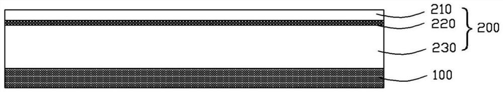
[0063] S1. Provide an epitaxial substrate 100; the epitaxial substrate 100 includes a sapphire patterned substrate, a sapphire substrate, a gallium nitride substrate, an aluminum nitride substrate, a silicon carbide substrate or a silicon substrate, etc., in this embodiment Among them, the epitaxial substrate 100 is specifically a sapphire patterned substrate or a sapphire flat substrate;

[0064] S2, such as figure 2As shown, a semiconductor epitaxial layer 200 is formed on an epitaxial substrate 100; the semiconductor epitaxial layer 100 includes a first type semiconductor layer 210, an active region 220 and a second type semiconductor layer 230 from top to bottom. In this embodiment, The first type semiconductor layer 210 is a P-type semiconductor layer, the second type semiconductor layer 230 is an N-type s...

Embodiment 2

[0076] The same example of this embodiment provides a method for manufacturing a light-emitting diode device. The similarities between this embodiment and Embodiment 1 will not be repeated. The difference is that the first groove 240, the second groove 250 and the third groove The etching sequence of the groove 260 is different, specifically:

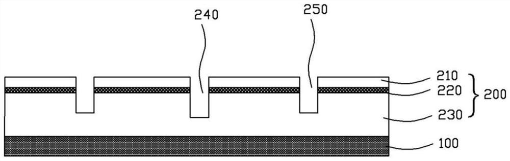
[0077] In step S3, the semiconductor epitaxial layer 200 is etched, the semiconductor epitaxial layer 200 includes a light emitting region and a cutting region between the light emitting regions, and the semiconductor epitaxial layer 200 is etched between the light emitting region and the cutting region of the semiconductor epitaxial layer 200 The third groove 260, the third groove 260 independently divides the semiconductor epitaxial layer 200 into a light emitting diode mesa 280 located in the light emitting area and a cutting area mesa 270 located in the cutting area, and the light emitting diode mesa 280 and the cutting area mesa 270...

Embodiment 3

[0081] This embodiment has multiple same features as Embodiment 1 or Embodiment 2, and the difference between this embodiment and Embodiment 1 or Embodiment 2 is:

[0082] Step S7: Do not etch or partially etch the semiconductor epitaxial layer 200 of the mesa 270 in the cutting area, and retain the semiconductor epitaxial layer 200 at the cutting line 241 or in the space between the cutting line 241 and the light emitting region. Here, for the same The characteristics are no longer described one by one, only the differences are described.

[0083] An embodiment of the present invention provides a method for fabricating a light emitting diode device. In step S7, the epitaxial substrate 100 is removed, and a third layer penetrating through the semiconductor epitaxial layer 200 is etched between the light emitting region and the cutting region of the semiconductor epitaxial layer 200. Groove 260, the third groove independently divides the semiconductor epitaxial layer 200 into a...


PUM

PropertyMeasurementUnit
heightaaaaaaaaaa
heightaaaaaaaaaa

Abstract

The invention discloses a light-emitting diode device and a preparation method thereof, which are not only suitable for light-emitting diode devices with a vertical structure, but also for other series of light-emitting diode devices such as a horizontal structure and a high-voltage structure. The light emitting diode device includes a substrate and a plurality of mesa structures located on the upper surface of the substrate. The mesa structure includes a light emitting diode mesa located in a light emitting area and a cutting area mesa located in a cutting area. The light emitting diode mesaand the cutting area mesa are arranged at intervals, and the cutting area Including the cutting channel and the spacer area, the reflective metal layer, the sacrificial layer and the first insulatinglayer inside the cutting channel are distributed in a trapezoid shape. This trapezoidal distribution method effectively improves the continuous direction of the stress at the cutting channel and reduces the continuous accumulation of stress Therefore, the stress lines and the abnormalities of easy peeling and falling off of the semiconductor epitaxial layer are reduced or eliminated, and the appearance yield of the light emitting diode device can be effectively improved, and the product quality of the light emitting diode device can be improved.

Description

technical field [0001] The invention relates to the related technical field of light emitting diodes, in particular to a light emitting diode device and a preparation method thereof. Background technique [0002] Existing light-emitting diode devices are widely used in many fields due to their high luminous efficiency. Light-emitting diode devices generally include epitaxial substrates, semiconductor epitaxial layers, sacrificial layers, insulating layers, metal layers and substrates. However, the existing light-emitting diode devices have differences in thermal expansion coefficient between the semiconductor epitaxial layer and the metal layer and substrate, differences in the thickness of the semiconductor epitaxial layer and growth temperature, and differences in the thickness of the metal layer. These differences in the light-emitting diode devices will make the light-emitting diode device Stress of different sizes is generated in the structure; in addition, the semicond...

Claims


Application Information

Patent Timeline
Patent Type & Authority Applications(China)
IPC IPC(8): H01L33/20H01L33/12H01L33/00
CPCH01L33/20H01L33/12H01L33/0095H01L33/0066H01L33/0093H01L2933/0016H01L33/382H01L27/156
Inventor 蔡琳榕杨力勋曾信义朱立钦
Owner XIAMEN SANAN OPTOELECTRONICS TECH CO LTD
Why Eureka
Try Eureka