Hydrogen sensor of gallium nitride-based high-electron-mobility transistor

A high electron mobility, gallium nitride-based technology, applied in the field of gas sensors, can solve the problems of harsh working conditions, inability to be widely used in various environments, weak output signals, etc., and achieve stable preparation, good performance, and simple operation. Effect

Inactive Publication Date: 2021-02-09
DALIAN UNIV OF TECH
View PDF6 Cites 3 Cited by
  • Summary
  • Abstract
  • Description
  • Claims
  • Application Information

AI Technical Summary

Problems solved by technology

The traditional hydrogen sensor is mainly resistive type, although its sensitivity is high, but its output signal is weak, so it is necessary t

Method used


Image

  • Hydrogen sensor of gallium nitride-based high-electron-mobility transistor
  • Hydrogen sensor of gallium nitride-based high-electron-mobility transistor
  • Hydrogen sensor of gallium nitride-based high-electron-mobility transistor

Examples


Embodiment 1

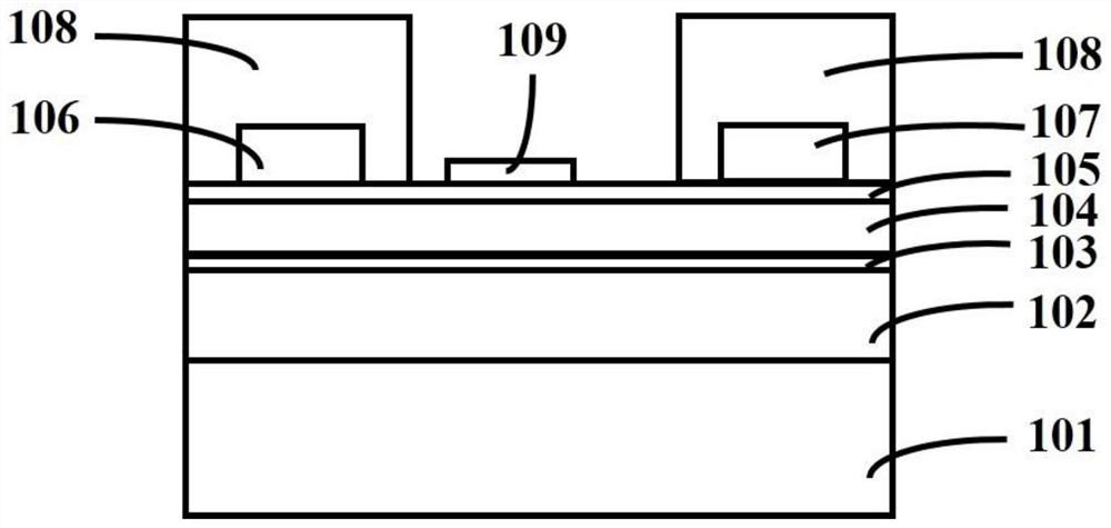
[0021] The HEMT structure used in the present invention is as figure 1 shown, including substrate 101 as Al 2 o 3 layer, 3 μm undoped GaN layer 102, 2 nm AlN intercalation layer 103, Al content 25%, 25 nm thick AlGaN layer 104, 2 nm thick GaN cap layer 105, Ti / Al / Ni / Au source electrode 106 and drain electrode 107, SiO 2 The electrode protective layer 108;

[0022] Specific steps are as follows:

[0023] Step 1: Surface pretreatment of HEMT epitaxial wafers: put the cut epitaxial wafers into acetone solution for ultrasonic cleaning for 10 minutes, take out the epitaxial wafers, put them into absolute ethanol for ultrasonic cleaning for 10 minutes, and then put the epitaxial wafers into deionized water for ultrasonic cleaning Wash for 10 minutes to remove the glue on the surface of the epitaxial wafer and organic matter attached to the surface; then take out the epitaxial wafer and soak it in a dilute hydrochloric acid solution with a volume ratio of 1:10 for 3 minutes to r...

Embodiment 2

[0028] The HEMT structure used in the present invention is as figure 1 shown, including substrate 101 as Al 2 o 3 layer, 3 μm undoped GaN layer 102, 2 nm AlN intercalation layer 103, Al content 25%, 25 nm thick AlGaN layer 104, 2 nm thick GaN cap layer 105, Ti / Al / Ni / Au source electrode 106 and drain electrode 107, SiO 2 The electrode protective layer 108;

[0029] Specific steps are as follows:

[0030] Step 1: Surface pretreatment of HEMT epitaxial wafers: put the cut epitaxial wafers into acetone solution for ultrasonic cleaning for 10 minutes, take out the epitaxial wafers, put them into absolute ethanol for ultrasonic cleaning for 10 minutes, and then put the epitaxial wafers into deionized water for ultrasonic cleaning Wash for 10 minutes to remove the glue on the surface of the epitaxial wafer and organic matter attached to the surface; then take out the epitaxial wafer and soak it in a dilute hydrochloric acid solution with a volume ratio of 1:10 for 3 minutes to r...

Embodiment 3

[0035] The HEMT structure used in the present invention is as figure 1 shown, including substrate 101 as Al 2 o 3 layer, 3 μm undoped GaN layer 102, 2 nm AlN intercalation layer 103, Al content 25%, 25 nm thick AlGaN layer 104, 2 nm thick GaN cap layer 105, Ti / Al / Ni / Au source electrode 106 and drain electrode 107, SiO 2 The electrode protective layer 108;

[0036] Specific steps are as follows:

[0037] Step 1: Surface pretreatment of HEMT epitaxial wafers: put the cut epitaxial wafers into acetone solution for ultrasonic cleaning for 10 minutes, take out the epitaxial wafers, put them into absolute ethanol for ultrasonic cleaning for 10 minutes, and then put the epitaxial wafers into deionized water for ultrasonic cleaning Wash for 10 minutes to remove the glue on the surface of the epitaxial wafer and organic matter attached to the surface; then take out the epitaxial wafer and soak it in a dilute hydrochloric acid solution with a volume ratio of 1:10 for 3 minutes to r...


PUM

PropertyMeasurementUnit
Thicknessaaaaaaaaaa
Thicknessaaaaaaaaaa

Abstract

The invention belongs to the technical field of gas sensors, and provides a hydrogen sensor of a gallium nitride-based high electron mobility transistor. A source electrode, a drain electrode and a Pd/Pt layer are respectively evaporated on the surface of a gallium nitride-based material. When hydrogen is adsorbed on a Pd/Pt layer and decomposed into hydrogen atoms to be transmitted to an interface, an electric field generated after the hydrogen atoms are subjected to interface polarization adsorption causes surface longitudinal charge change, then the two-dimensional electron gas concentration at a heterojunction interface is modulated, the output current of a source electrode and a drain electrode is changed, and therefore hydrogen concentration is tested. The preparation method is advantaged in that operation is simple, the prepared hydrogen sensor is good in stability, low in cost and the like, the prepared hydrogen sensor is good in quality, good performance can be kept, the hydrogen sensor can be tested in a loose humidity environment, and the output of the hydrogen sensor cannot be influenced. The preparation environment condition requirement is simple, and stable preparation can be realized.

Description

technical field [0001] The invention belongs to the technical field of gas sensors, and in particular relates to a hydrogen gas sensor of a gallium nitride-based high electron mobility transistor. Background technique [0002] As the world's demand for energy continues to increase, the consumption of fossil energy continues to increase, which has a more adverse impact on the environment. Therefore, people are eager to increase the proportion of renewable energy in the energy structure, and hydrogen is given high hopes as a renewable energy. At the same time, hydrogen has a wide range of applications in the fields of aerospace, weapon systems, medical health, and fuel cells. However, when the hydrogen content in the local air is between 4% and 90%, an explosion will occur, and because the hydrogen molecule is very small, it is easy to leak during the actual production and transportation, and the hydrogen molecule is colorless and tasteless. It is not easy to be detected, an...

Claims


Application Information

Patent Timeline
IPC IPC(8): G01N27/414H01L29/66H01L29/778
CPCG01N27/4141H01L29/66431H01L29/778
Inventor 张贺秋杨勇强梁红伟夏晓川
Owner DALIAN UNIV OF TECH
Why Eureka
Try Eureka