

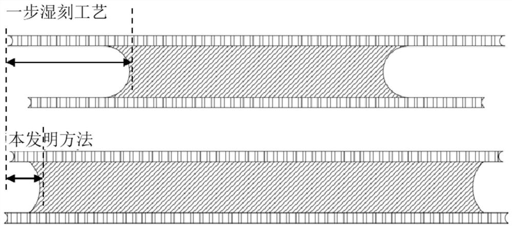
Method for preparing high-precision silver electrode by side wall protection process
A sidewall protection, high-precision technology, applied in circuits, electrical components, electrical solid-state devices, etc., can solve the problems of inability to apply Ag electrode structure, large AgCDloss, poor aluminum conductivity, etc., to meet the needs of ultra-high-resolution display , The effect of reducing CDloss
- Summary
- Abstract
- Description
- Claims
- Application Information
AI Technical Summary
Problems solved by technology
Method used
Image

Examples
Embodiment 1
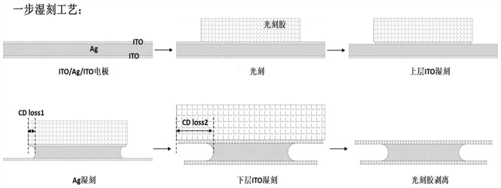
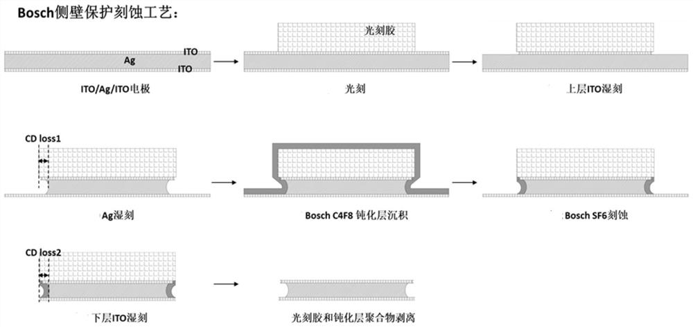
[0034] A method for preparing a high-precision silver electrode by a sidewall protection process, comprising the following steps:
[0035] 1) The ITO / Ag / ITO structure is a three-layer sandwich structure, which is ITO layer, Ag layer and ITO layer from bottom to top, and its thickness is 100A, 1000A, 100A from bottom to top; photolithography is performed first, and PR Thickness 1μm, curing energy 50mj;
[0036] 2), then wet etching the upper layer ITO not protected by the photoresist, using 8wt% oxalic acid etching, time 20s to remove the upper layer ITO, and then wet etching the Ag layer with nitric acid / phosphoric acid / acetic acid mixture for 10s to remove the Ag layer; Nitric acid / phosphoric acid / acetic acid mixture, the mass fraction ratio is 20%:40%:40%.
[0037] 3), and then proceed to C 4 f 8 Deposit passivation layer, process parameters: time 10s, power supply power 300W, C 4 f 8 The flow rate is 10sccm, the pressure is 5mt, and the temperature is 50°C; it is used ...
Embodiment 2
[0043] A method for preparing a high-precision silver electrode by a sidewall protection process, comprising the following steps:
[0044] 1) The ITO / Ag / ITO structure is a three-layer sandwich structure, and its thickness is 500A, 5000A, and 500A in turn; for photolithography, the PR thickness is 2μm, and the curing energy is 500mj;
[0045] 2) Remove the upper layer of ITO at the position not protected by the photoresist, use 4wt% oxalic acid wet etching for 50s, remove the upper layer of ITO; then perform Ag wet etching, nitric acid / phosphoric acid / acetic acid mixed solution wet etching for 20s, remove the Ag layer; The nitric acid / phosphoric acid / acetic acid mixed acid used has a mass fraction ratio of 30%:30%:40%.
[0046] 3), C 4 f 8 Deposit passivation layer, process parameters: time 30s, power supply power 500W, C 4 f 8 The flow rate is 20sccm, the pressure is 10mt, and the temperature is 50°C. Both the photoresist surface and the exposed Ag surface area on the und...
PUM
| Property | Measurement | Unit |
|---|---|---|
| Layer thickness | aaaaa | aaaaa |
| Curing energy | aaaaa | aaaaa |
Abstract
Description
Claims
Application Information