Flat insertion type electronic probe and detection method

A flat plug-in, electronic technology, applied in the direction of measuring devices, material analysis using wave/particle radiation, instruments, etc., can solve problems such as poor spatial resolution, difficult electron beam focusing, large working distance, etc., to achieve spatial resolution High rate, overcome the effect of small representation space

Pending Publication Date: 2021-02-19
CHONGQING UNIV
View PDF0 Cites 1 Cited by
  • Summary
  • Abstract
  • Description
  • Claims
  • Application Information

AI Technical Summary

Problems solved by technology

[0003] 1) poor spatial resolution
[0004] In the traditional EBSD working mode, the working distance is relatively large, generally around 10-15mm, it is difficult to focus the electron beam to the smallest size, and the spatial resolution is not high
At the same time, because the normal direction of the sample surface forms an angle of 70° with the electron beam, the circular beam spot is elongated into an ellipse, and the spatial resolution in one direction drops by 3 times;
[0005] 2) Smaller sample movement range
If the sample stage movement mode is used for EBSD scanning in a large size range, it is easy to hit the probe
Therefore, EBSD characterization of large-scale samples cannot be performed in this working mode;
[0007] 3) Not easily correlated with backscattered electron images
However, switching between the EBSD probe and the BSE probe requires the sample to be tilted in a large range, which is extremely inconvenient to use. For samples with small grain sizes, there are also big problems in the positioning of the sample area.

Method used


Image

  • Flat insertion type electronic probe and detection method
  • Flat insertion type electronic probe and detection method

Examples


Embodiment Construction

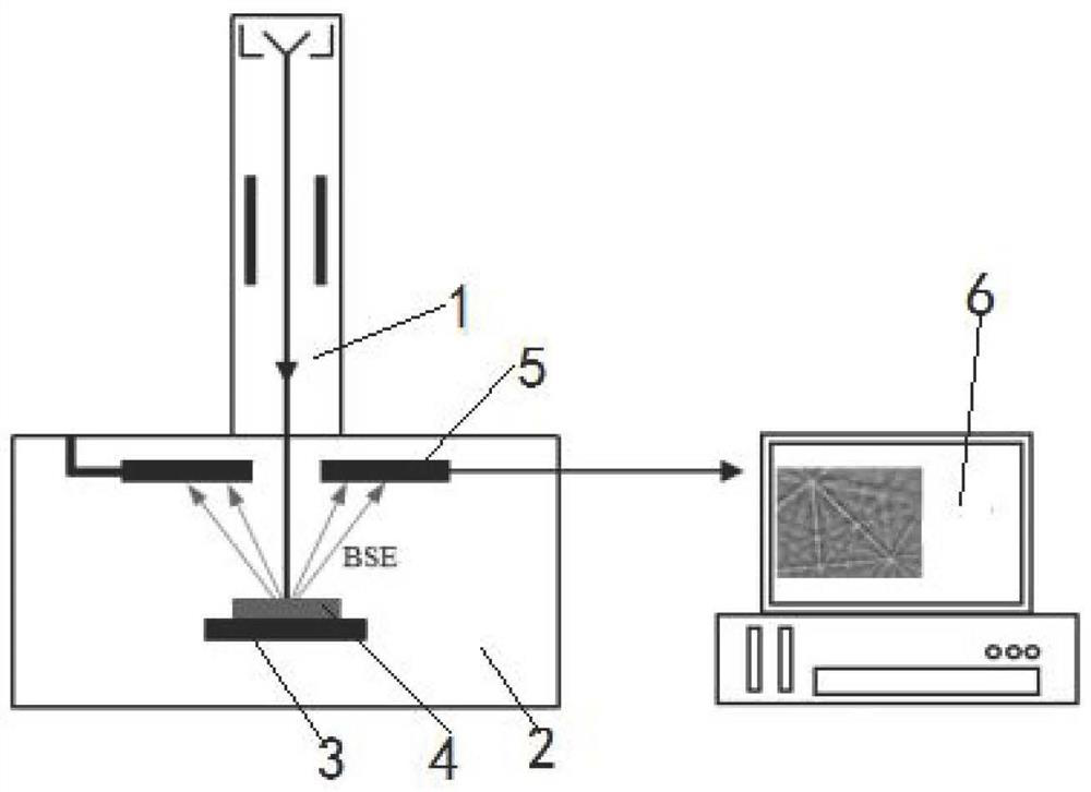
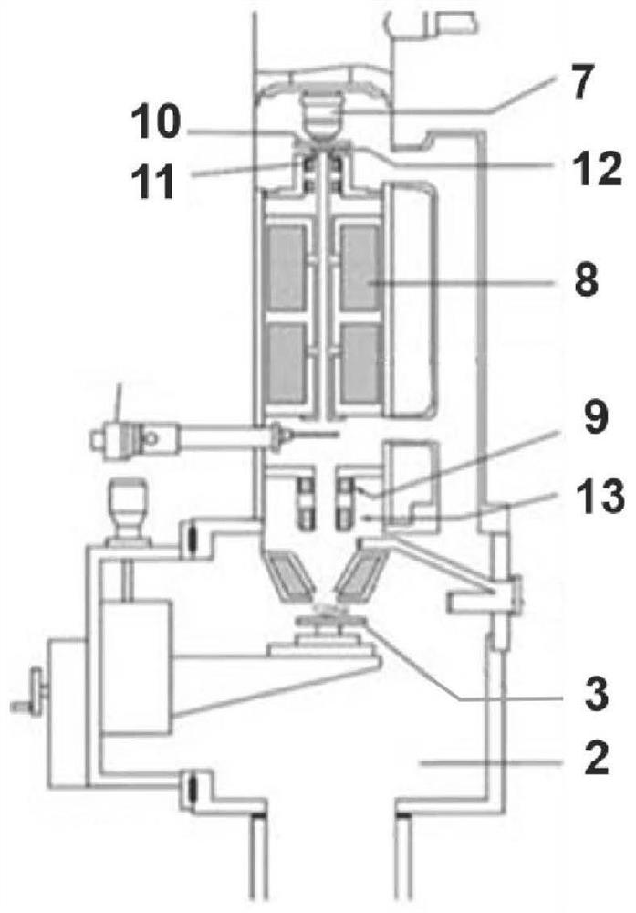
[0028] The specification and claims do not use the difference in name as a way to distinguish components, but use the difference in function of components as a criterion for distinguishing. As mentioned throughout the specification and claims, "comprising" is an open term, so it should be interpreted as "including but not limited to". "Approximately" means that within an acceptable error range, those skilled in the art can solve the technical problem within a certain error range and basically achieve the technical effect.

[0029] The orientation terms such as up, down, left, and right in this specification and claims are combined with the drawings for further explanation, making this application easier to understand, and not limiting this application. In different scenarios, up and down, left and right, and inside and outside are all Relatively speaking.

[0030] The present invention will be described in further detail below in conjunction with the accompanying drawings.

...


PUM


Abstract

The invention discloses a flat insertion type electronic probe, and relates to the technical field of electron microscopic imaging technology and metal material crystallography characterization. The flat insertion type electronic probe has higher spatial resolution, supports large-range movement of a sample, and can directly obtain a back scattering electron image and improve applicability of a large-size sample and the convenience of combined use with an ECCI technology; According to the specific scheme, the flat insertion type electronic probe comprises an electron gun, a transmission channel, a sample chamber, a signal reading device and a signal receiving device; the electron gun is used for emitting electron beams, the electron beams enter the sample chamber through the transmission channel, a sample table is arranged in the sample chamber, the sample table is used for containing samples, the electron beam irradiates a sample and carries out backscattering, the signal reading device is used for receiving the electron beam backscattered by the sample stage, the signal reading device is a CCD camera, and the CCD camera is in data connection with the signal receiving device. Theflat insertion type electronic probe provided by the invention is high in spatial resolution, and the working distance of the direct insertion type EBSD probe is smaller.

Description

technical field [0001] The invention relates to the technical fields of electron microscopic imaging technology and crystallographic characterization of metal materials, more specifically, it relates to a flat insertion type electronic probe and a detection method. Background technique [0002] Since the invention of Electron backscatter diffraction (EBSD) in the 1990s, it has made great achievements in the field of microstructure characterization (such as phase identification and phase distribution, grain boundary characteristics, grain morphology, micro-texture analysis, etc.). Great development, now widely used. In the traditional EBSD test system, the angle between the electron beam and the sample surface is 70°, and the cylindrical probe extends from the side to receive the backscattered electron signal. This mode can obtain a very good Kikuchi pattern signal. But there are following problems: [0003] 1) poor spatial resolution [0004] In the traditional EBSD worki...

Claims


Application Information

Patent Timeline
Patent Type & Authority Applications(China)
IPC IPC(8): G01N23/203G01N23/205G01N23/20058G01N23/20025
CPCG01N23/20025G01N23/20058G01N23/203G01N23/205G01N2223/053G01N2223/0561G01N2223/0565G01N2223/102G01N2223/501
Inventor 黄天林黄小愉吴桂林
Owner CHONGQING UNIV
Why Eureka
Try Eureka