Supercharge Your Innovation With Domain-Expert AI Agents!

Apparatus and method for reducing access device sub-threshold leakage in semiconductor device

A technology of equipment and storage body, which is applied in the direction of information storage, static storage, digital storage information, etc., and can solve the problems of reduced reliability of storage devices and affecting units

Pending Publication Date: 2021-02-23
MICRON TECH INC
View PDF0 Cites 0 Cited by
  • Summary
  • Abstract
  • Description
  • Claims
  • Application Information

AI Technical Summary

Problems solved by technology

This increase in the IOFF leakage of the access device may lead to a decrease in the reliability of the memory device
For example, when a sense amplifier drives a bit line to a '0', it may affect a cell storing data '1'
This increase in access device IOFF leakage has limited further scaling of the memory cell

Method used


Image

  • Apparatus and method for reducing access device sub-threshold leakage in semiconductor device
  • Apparatus and method for reducing access device sub-threshold leakage in semiconductor device
  • Apparatus and method for reducing access device sub-threshold leakage in semiconductor device

Examples


Embodiment Construction

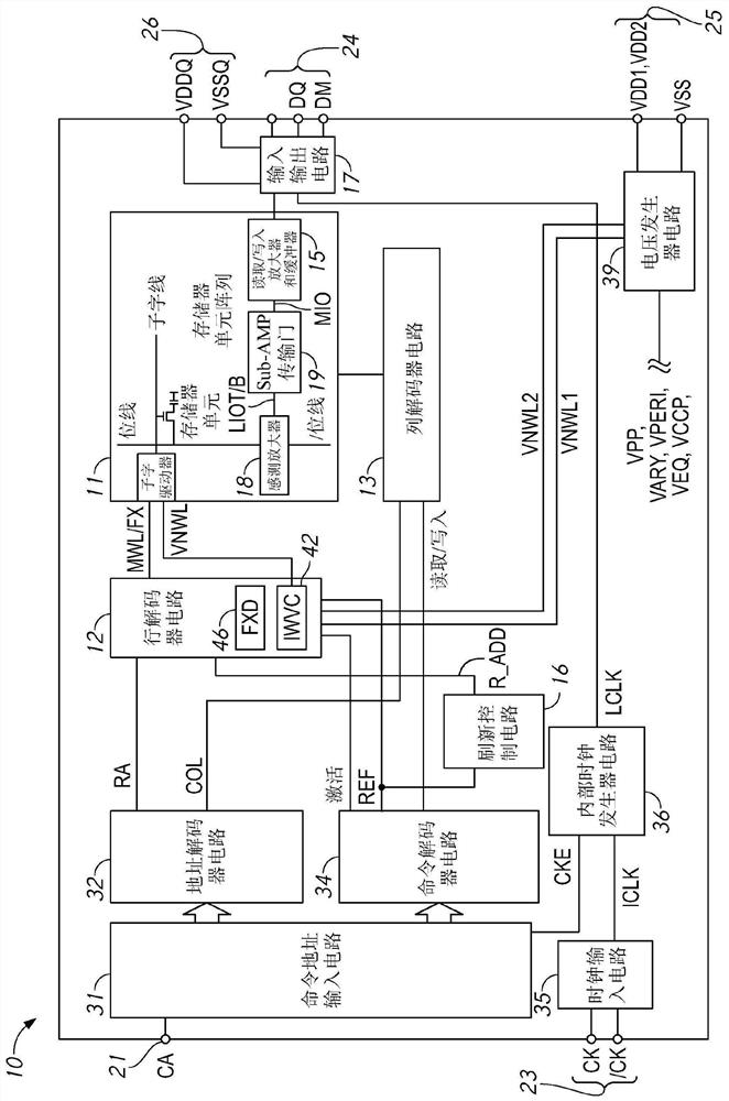
[0016] Certain details are set forth below in order to provide a thorough understanding of examples of various embodiments of the present disclosure. However, it is understood that the examples described herein may be practiced without these specific details. Furthermore, specific examples of the disclosure described herein should not be construed to limit the scope of the disclosure to those specific examples. In other instances, well-known circuits, control signals, timing schemes and software operations have not been shown in detail in order to avoid unnecessarily obscuring the embodiments of the present disclosure. Additionally, terms such as "couples / coupled" mean that two components may be electrically coupled, directly or indirectly. Indirect coupling can imply that two components are coupled through one or more intermediate components.

[0017] A semiconductor memory device may include main word lines and sub word lines in a hierarchical structure. The main word lin...


PUM


Abstract

The invention relates to an apparatus and method for reducing access device sub-threshold leakage in a semiconductor device. In some examples, a non-active word line voltage control (IWVC) circuit maybe configured to provide a non-active potential (from a default off-state word line voltage (VNWL) to a reduced voltage (VNWL) that is lower than the default VNWL) to a respective sub-word driver associated with one of a plurality of banks after a certain duration after activating the bank. The IWVC circuit may also be configured to provide the default VNWL to a respective sub-word driver in response to pre-charging the bank. The IWVC circuit may include a multiplexer coupled to the sub-word drivers and configured to provide the default VNWL or the reduced voltage VNWL to the respective sub-word drivers in response to a VNWL control signal. The IWVC circuit may also include a time control circuit configured to provide the VNWL control signal in response to a clock signal and a time control signal.

Description

technical field [0001] The present disclosure relates to semiconductor devices, and more particularly to apparatus and methods for reducing access device subthreshold leakage in semiconductor devices Background technique [0002] A semiconductor memory device such as a DRAM (Dynamic Random Access Memory) includes a memory cell array having memory cells arranged at intersections between word lines and bit lines. A semiconductor memory device may include main word lines and sub word lines in a hierarchical structure. The main word line is the word line located in the upper layer, and is selected by the first part of the row address. A sub word line is a word line located in a lower layer, and is selected based on a corresponding main word line (MWL) and a word driver line (FX) selected by the second part of the row address. [0003] Due to scaling of array access devices in semiconductor fabrication (eg, smaller pitch dimensions of transistor circuits and need to rebalance i...

Claims


Application Information

Patent Timeline
Patent Type & Authority Applications(China)
IPC IPC(8): G11C11/408G11C11/4097
CPCG11C11/4085G11C11/4097G11C5/025G11C8/14G11C8/08G11C2207/005G11C11/4076G11C7/222G11C8/12G11C11/4087G11C8/18G11C8/10G11C11/406
Inventor B·H·拉姆S·M·希尔德K·L·马约尔T·马利
Owner MICRON TECH INC
Features
  • R&D
  • Intellectual Property
  • Life Sciences
  • Materials
  • Tech Scout
  • Unparalleled Data Quality
  • Higher Quality Content
  • 60% Fewer Hallucinations
Learn More