Semiconductor device and manufacturing method thereof

A manufacturing method and semiconductor technology, applied in the direction of semiconductor devices, electrical solid devices, electrical components, etc., can solve the problems of affecting the normal use of three-dimensional memory devices, prone to sharp corners, insufficient filling, etc., and achieve the weakening of stress or electron attraction. Force action, avoid leakage, avoid the effect of connecting the upper and lower gate layers

Active Publication Date: 2021-02-23
YANGTZE MEMORY TECH CO LTD
View PDF3 Cites 4 Cited by
  • Summary
  • Abstract
  • Description
  • Claims
  • Application Information

AI Technical Summary

Problems solved by technology

Virtual channel holes are usually designed to be circular, but in the process of making virtual channel holes, sharp corners are prone to occur. When filling virtual channel holes later, the sharp corners may be insufficiently filled and produce Larger gaps lead to the subsequent filling of tungsten to form the gate layer, the upper and lower gate layers are connected, resulting in leakage of three-dimensional memory devices, affecting the normal use of three-dimensional memory devices

Method used


Image

  • Semiconductor device and manufacturing method thereof
  • Semiconductor device and manufacturing method thereof
  • Semiconductor device and manufacturing method thereof

Examples


Embodiment 1

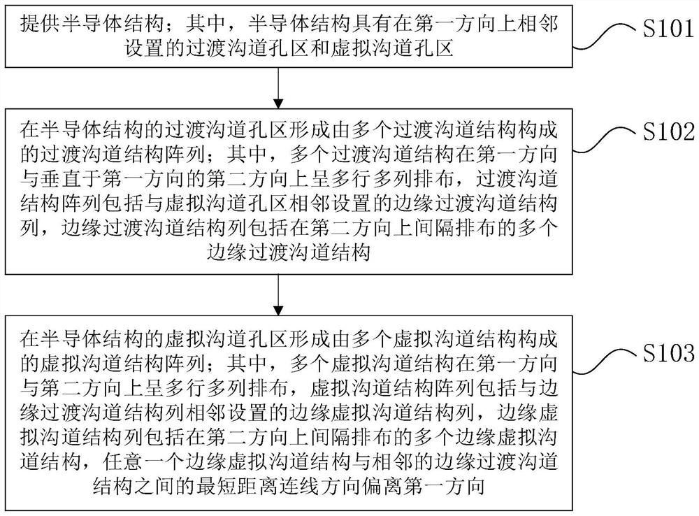
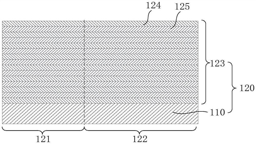
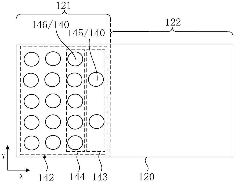
[0074] Such as figure 1 S101 in figure 2 and image 3 As shown, a semiconductor structure 120 is provided; wherein, the semiconductor structure 120 has a transition channel region 121 and a dummy channel region 122 adjacently arranged in a first direction.

[0075] Specifically, the semiconductor structure 120 includes a substrate 110 and a stack structure 123 on the substrate 110 . The first direction in this embodiment is the X direction in the figure, and the first direction is parallel to the upper surface of the substrate 110 , and the upper surface of the substrate 110 is a surface in contact with the stacked structure 123 .

[0076] The substrate 110 may include a silicon substrate, a germanium (Ge) substrate, a silicon germanium (SiGe) substrate, an SOI substrate, or a GOI (Germanium-on-Insulator, germanium-on-insulator) substrate and the like. In other embodiments, the substrate 110 may also be a substrate including other element semiconductors or compound semicon...

Embodiment 2

[0110] Such as Figure 11 As shown, the embodiment of the present application also provides a semiconductor device 100 ′, which is different from the first embodiment above in that the multiple non-edge transition channel structures 135 in any two adjacent non-edge transition channel structure columns 134 are arranged alternately in sequence in the second direction. Moreover, a plurality of non-edge dummy channel structures 155 in any two adjacent non-edge dummy channel structure columns 154 are sequentially arranged alternately in the second direction, and are close to the non-edge dummy channel structures 152 of the edge dummy channel structure column 152. The plurality of non-edge dummy channel structures 155 and the plurality of edge dummy channel structures 153 in the channel structure column 154 are sequentially arranged alternately in the second direction.

[0111] Since the other structures of the semiconductor device 100' in the embodiment of the present application ...


PUM


Abstract

The invention discloses a semiconductor device and a manufacturing method thereof. The semiconductor device comprises a semiconductor structure, a transition channel structure array and a virtual channel structure array, wherein the transition channel structure array and the virtual channel structure array are arranged in the semiconductor structure and are adjacently arranged in a first direction; the transition channel structure array comprises an edge transition channel structure column adjacent to the virtual channel structure array, the edge transition channel structure column comprises aplurality of edge transition channel structures arranged at intervals in the second direction, and the second direction is perpendicular to the first direction; the virtual channel structure array comprises an edge virtual channel structure column adjacent to the edge transition channel structure column, and the edge virtual channel structure column comprises a plurality of edge virtual channel structures arranged at intervals in the second direction; the shortest distance connecting line direction between any edge virtual channel structure and the adjacent edge transition channel structure deviates from the first direction. The problem of sharp corners of the edge virtual channel holes can be avoided, and therefore electric leakage of the three-dimensional storage device is avoided.

Description

technical field [0001] The present application relates to the technical field of semiconductors, in particular to a semiconductor device and a manufacturing method thereof. Background technique [0002] In the fabrication process of a three-dimensional memory, in addition to designing device channel holes, transition channel holes and dummy channel holes are often designed to achieve related functions, such as providing structural support during the subsequent silicon nitride removal process. The virtual channel hole is usually designed to be circular, but in the process of making the virtual channel hole, it is easy to have a sharp corner problem. When filling the virtual channel hole later, the sharp corner may be insufficiently filled and produce Larger gaps will cause the upper and lower gate layers to be connected when the gate layer is subsequently filled with tungsten, which will cause leakage of the three-dimensional memory device and affect the normal use of the thr...

Claims


Application Information

Patent Timeline
Patent Type & Authority Applications(China)
IPC IPC(8): H01L27/11565H01L27/1157H01L27/11582
CPCH10B43/35H10B43/10H10B43/27
Inventor 刘隆冬
Owner YANGTZE MEMORY TECH CO LTD
Why Eureka
Try Eureka