Semiconductor structure preparation method and semiconductor device

A semiconductor and device technology, which is applied in the field of semiconductor structure preparation methods and semiconductor devices, and can solve problems such as extremely high process temperature requirements, lack of availability, and complexity

Active Publication Date: 2021-02-26
NANJING UNIV
View PDF7 Cites 0 Cited by
  • Summary
  • Abstract
  • Description
  • Claims
  • Application Information

AI Technical Summary

Problems solved by technology

However, at present, three-dimensional complementary devices are mainly prepared by N-type transistors on top of P-type transistors. This process not only requires extremely high temperature for subsequent processes, but also is relatively complicated.
This problem can be solved if nanowires with different doping types can be integrated simultaneously in three dimensions, but no such technology has been disclosed so far.

Method used


Image

  • Semiconductor structure preparation method and semiconductor device
  • Semiconductor structure preparation method and semiconductor device
  • Semiconductor structure preparation method and semiconductor device

Examples


Embodiment 1

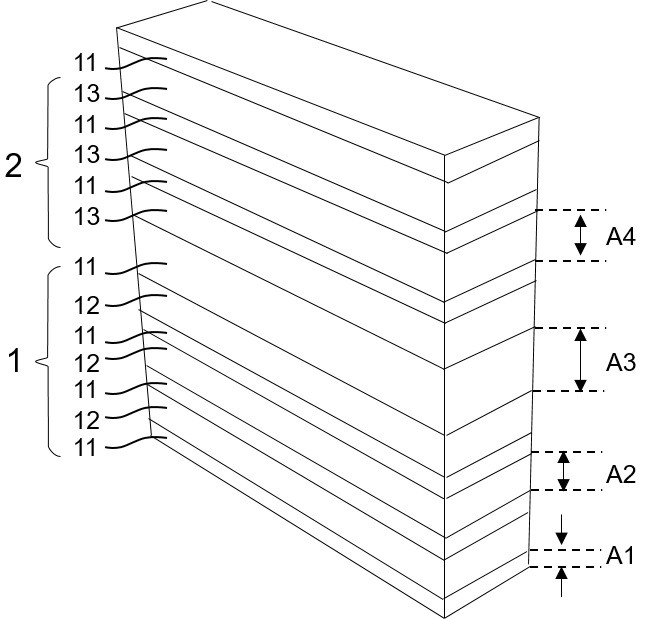
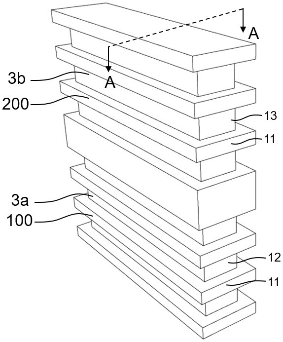
[0043] This embodiment first provides a method for simultaneously integrating P-type and N-type stacked nanowires in a three-dimensional direction, such as Figure 1a~1i As shown, the method includes at least the following steps:

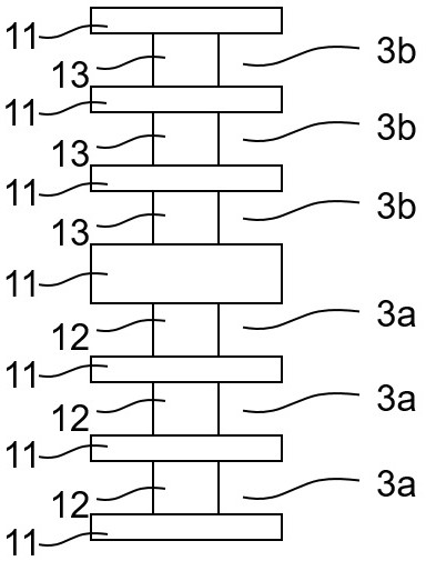
[0044] The first step is to alternately deposit the first thin film layer 11 and the second thin film layer 12 to form the first base material layer 1; continue to alternately deposit the first thin film layer 11 and the third thin film layer 13 on the first base material layer to form The second base material layer 2 is formed.

[0045] The substrate layer is patterned to expose the first sidewall 100 of the first substrate layer in the stacking direction and the second sidewall 200 of the second substrate layer in the stacking direction. Using SF 6 or C 4 f 8 or CF 4 and other fluorine-containing plasma etching methods, etch downward along the edge of the pattern, etch the first and third film layers except the pattern coverage area, exposing...


PUM

PropertyMeasurementUnit
diameteraaaaaaaaaa
thicknessaaaaaaaaaa
thicknessaaaaaaaaaa

Abstract

The invention discloses a semiconductor structure preparation method comprising the following steps that: step 1, a first substrate layer and a second substrate layer are formed, wherein the first substrate layer is composed of a first thin film layer and a second thin film layer which are alternately deposited, and the second substrate layer is composed of a first thin film layer and a third thinfilm layer which are alternately deposited on the first substrate layer; the first thin film layer is a silicon oxide or silicon nitride thin film, the second thin film layer is an intrinsic or P-type amorphous layer, the third thin film layer is an N-type amorphous layer, a first groove is etched in the second thin film layer, and a second groove is etched in the third thin film layer.

Description

technical field [0001] The invention relates to a method for preparing a semiconductor structure and a semiconductor device, in particular to a method for simultaneously integrating P-type and N-type stacked nanowires in a three-dimensional direction and a semiconductor device prepared by the method, belonging to the field of microelectronic technology. Background technique [0002] With the continuous miniaturization of devices, the structure of transistors has also changed from a traditional planar structure to a three-dimensional direction. After the 3nm process node, the large distance between P-type transistors and N-type transistors will become the main reason for hindering the further scaling of devices. Using the current partition doping process, the distance between PMOS and NMOS is about 300 nm. If the P-type Transistors and N-type transistors are stacked vertically to form three-dimensional complementary devices, which can break through this bottleneck. However, ...

Claims


Application Information

Patent Timeline
Patent Type & Authority Applications(China)
IPC IPC(8): H01L21/8238H01L29/06H01L29/10H01L27/092B82Y40/00
CPCH01L21/823807H01L27/092H01L29/1033H01L29/0673B82Y40/00
Inventor 余林蔚胡瑞金王军转
Owner NANJING UNIV
Why Eureka
Try Eureka