Chip packaging structure and electronic product

A chip packaging structure, chip packaging technology, applied in the direction of circuits, electrical components, electric solid devices, etc., can solve problems such as easy tilt deformation, poor bonding of plastic sealing mold surface, complicated operation, etc.

Active Publication Date: 2021-02-26
BYD SEMICON CO LTD
View PDF5 Cites 0 Cited by
  • Summary
  • Abstract
  • Description
  • Claims
  • Application Information

AI Technical Summary

Problems solved by technology

[0003] The DFN (Double Flat No-Leads) package shape product in the prior art is more and more widely used in the industry because of its advantages of smaller product size and thinner package thickness than other package shape products because of its no exposed pins. Use; the double-sided heat dissipation method of this kind of DFN package shape product is to paste the copper sheet on the chip, then paste the heat dissipation block on the copper sheet, and then plastic seal it. Uneven mounting surface, easy to tilt and deform after reflow soldering, resulting in uneven surface of heat sink, not tight fit with plastic mold surface, easy to generate flash, need to add flash removal and grinding processes, complex operation

Method used


Image

  • Chip packaging structure and electronic product
  • Chip packaging structure and electronic product
  • Chip packaging structure and electronic product

Examples


Embodiment Construction

[0034] Specific embodiments of the present disclosure will be described in detail below in conjunction with the accompanying drawings. It should be understood that the specific embodiments described here are only used to illustrate and explain the present disclosure, and are not intended to limit the present disclosure.

[0035] In this disclosure, unless stated otherwise, the orientation words used such as "upper and lower" refer to the upper and lower parts of the chip package structure installed in the electronic product and in the state of horizontal use, and the definitions of upper and lower The following are represented by A and B respectively, please refer to Image 6 shown. In addition, terms used such as "first", "second" and the like are only used to distinguish one element from another element, and do not have sequence or importance.

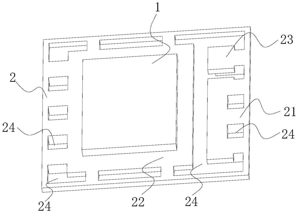
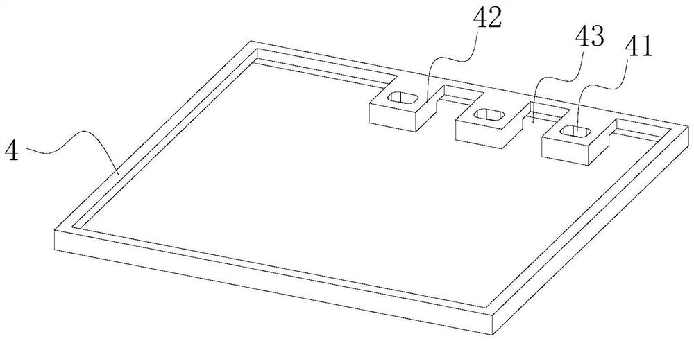
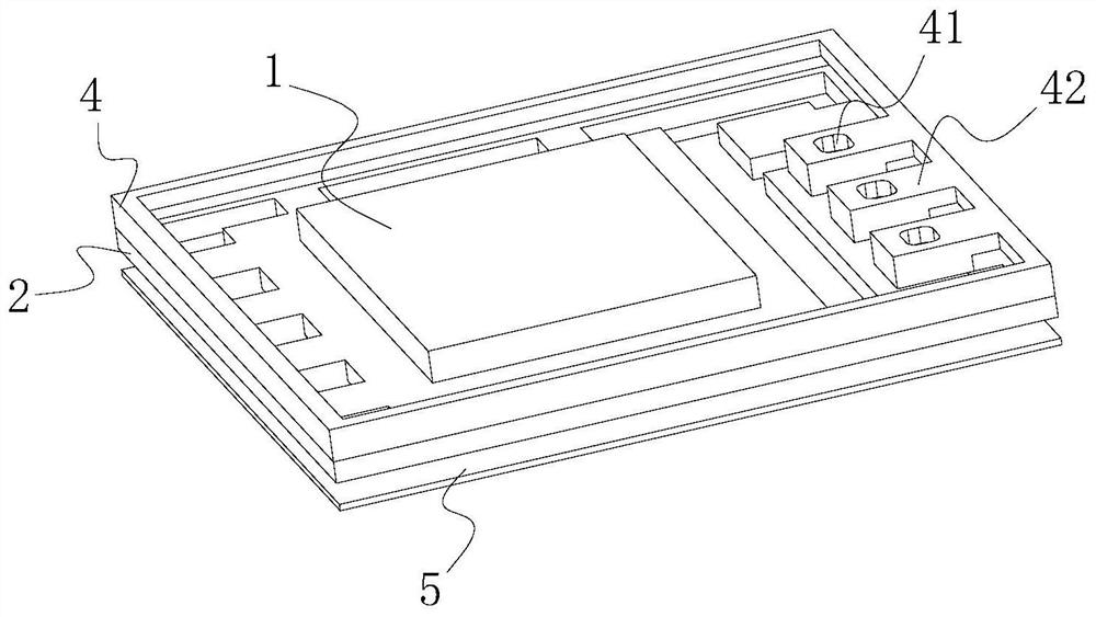
[0036] Such as Figure 1 to Figure 7 As shown, the present disclosure provides a chip packaging structure, which can be composed...


PUM


Abstract

The invention relates to a chip packaging structure and an electronic product. The chip packaging structure is composed of a plurality of chip packaging units, and each chip packaging unit comprises afirst lead frame, wherein power pins and a bearing platform are formed on the first lead frame, and the upper surface of the bearing platform is used for being fixedly connected with the lower surface of a chip; a second lead frame which is used for being fixed on the upper surface of the chip and is connected with the power pins; and a first half-etching groove and a second half-etching groove are respectively formed on the joint surfaces of the second lead frame and the chip and the power pins. The bonding material can be arranged in the first half-etching groove and the second half-etchinggroove without overflowing, so that the second lead frame is tightly attached to the upper surface of the chip and the power pins on the first lead frame, and the problem of inclination is avoided. Therefore, the problem of flash caused by untight fitting with the surface of the plastic package mold in the subsequent process is avoided, and processes of flash removal, grinding and the like are prevented from being added.

Description

technical field [0001] The present disclosure relates to the technical field of electronic products, and in particular, to a chip packaging structure and electronic products. Background technique [0002] With the diversified demands and development of electronic products, not only are the products required to be smaller and smaller, but also their functions are more powerful, especially low-power portable products. The power supply is a relatively large component in the system. If the product is to be made smaller, the power density of the power supply system must be high, small in size and high in power. The ensuing problem is that the space becomes smaller, and the heat generated inside cannot be dissipated, which can easily lead to damage to the power system. The main switching device in the power system is a low-voltage power MOSFET (metal-oxide semiconductor effect transistor). In order to reduce the size of the power system and output high power, it is necessary to i...

Claims


Application Information

Patent Timeline
Patent Type & Authority Applications(China)
IPC IPC(8): H01L23/495
CPCH01L23/49537H01L23/49551H01L2224/38H01L2224/40245H01L2224/32245
Inventor 吴彦李欢欢
Owner BYD SEMICON CO LTD
Why Eureka
Try Eureka