Blind hole electroplating filling method and circuit board

A technology of electroplating hole filling and circuit board, which is applied in the fields of printed circuit, printed circuit, printed circuit manufacturing, etc. It can solve the problems of affecting the quality of circuit board, uneven growth rate of hole wall plating, and insufficient hole filling of blind holes, etc., to achieve improved The effect of electroplating solution exchange efficiency, accelerated coating growth rate, and average coating growth rate

Active Publication Date: 2022-05-17
HUAIAN TECHUANG TECH CO LTD
View PDF6 Cites 0 Cited by
  • Summary
  • Abstract
  • Description
  • Claims
  • Application Information

AI Technical Summary

Problems solved by technology

[0005] 1. Due to the small aperture of the blind hole of the circuit board, copper ions are mostly located on the surface of the circuit board and the opening of the blind hole, and it is difficult to enter the inside of the blind hole, so the adhesion speed of copper ions on the surface of the board and around the hole is very high In the hole, that is, the growth rate of the coating on the surface of the circuit board is much greater than the growth rate of the coating on the wall of the blind hole, which eventually leads to voids in the hole and the transmission effect of the circuit board is seriously affected
[0006] 2. In order to avoid voids in the blind hole, the method of reducing the current density is usually used to reduce the growth rate of the coating, so that the copper ions have enough time to enter the blind hole, and then the copper ions can be more uniformly attached to the hole wall and the board surface, to achieve the effect of uniform growth of the plating layer on the board surface and the hole wall. However, this method greatly prolongs the plating time and reduces the efficiency of circuit board processing.
[0007] 3. It is difficult to accurately control the filling quality of blind holes
Due to the different concentration of copper ions in the blind holes, the growth rate of the plating layer on the hole wall is uneven during the electroplating process, and often some blind holes are not filled enough to cause depressions, or some blind holes are filled too much to form bulges. The situation affects the quality of the circuit board

Method used


Image

  • Blind hole electroplating filling method and circuit board
  • Blind hole electroplating filling method and circuit board
  • Blind hole electroplating filling method and circuit board

Examples


Embodiment Construction

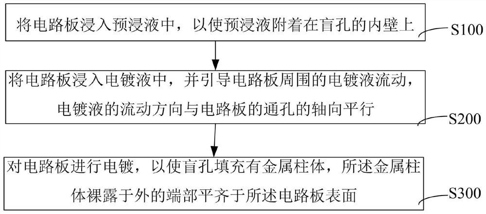
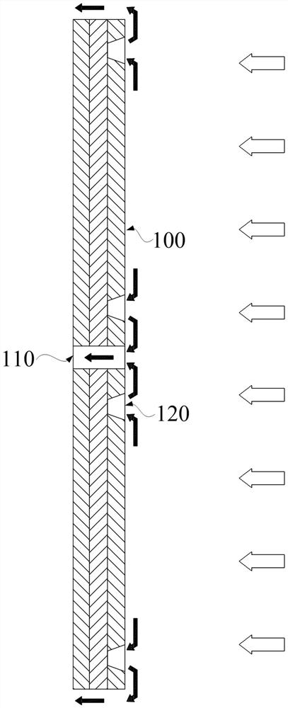
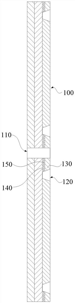
[0033] In order to facilitate understanding of the present invention, the present invention will be described more fully hereinafter with reference to the related drawings. The preferred embodiments of the invention are shown in the accompanying drawings. However, the present invention may be embodied in many different forms and is not limited to the embodiments described herein. Rather, these embodiments are provided so that a thorough and complete understanding of the present disclosure is provided.

[0034] It should be noted that when an element is referred to as being "fixed to" another element, it can be directly on the other element or intervening elements may also be present. When an element is referred to as being "connected" to another element, it can be directly connected to the other element or intervening elements may also be present. The terms "vertical", "horizontal", "left", "right" and similar expressions used herein are for the purpose of illustration only ...


PUM


Abstract

The present application provides a blind hole electroplating filling method and a circuit board. The above-mentioned blind hole electroplating and filling method is used to fill blind holes on a circuit board, and the blind hole electroplating and filling method includes the following steps: immersing the circuit board in a pre-dipping liquid, so that the pre-dipping liquid adheres to On the inner wall of the blind hole; the circuit board is immersed in the electroplating solution, and the electroplating solution around the circuit board is guided to flow, and the flow direction of the electroplating solution is in line with the axis of the through hole of the circuit board to be parallel; the circuit board is electroplated, so that the blind hole is filled with a metal column, and the exposed end of the metal column is flush with the surface of the circuit board. The electroplating hole filling method adopted in the present invention has the advantages of uniform plating growth rate on the surface of the circuit board and inside the blind hole, high electroplating and hole filling efficiency, and good blind hole filling effect.

Description

technical field [0001] The invention relates to the field of production and manufacture of printed circuit boards, in particular to a blind hole electroplating and filling method and a circuit board. Background technique [0002] High Density Interconnect Technology (HDI) is developed to meet the requirements of electronic products to be lighter, thinner, faster, and higher in frequency, and to meet the needs of miniaturization of micro devices and high density of packaging technology. A comprehensive and new type of manufacturing technology for electronic packaging carriers. In the early 1990s, Japan and the United States pioneered the application of high-density technology. After more than ten years of development, HDI boards have achieved considerable development. Especially in recent years, the pull of the domestic 3G mobile phone market has injected continuous development into HDI boards. power. [0003] Electroplating hole filling technology is currently the main tec...

Claims


Application Information

Patent Timeline
Patent Type & Authority Patents(China)
IPC IPC(8): H05K3/42H05K1/11
CPCH05K3/421H05K3/423H05K1/113H05K2201/09509H05K2201/0959
Inventor 许校彬
Owner HUAIAN TECHUANG TECH CO LTD
Why Eureka
Try Eureka