Plasma reaction device for improving uniform gas distribution

A plasma and reaction device technology, which is applied in the uniform distribution of ions and semiconductor equipment manufacturing, can solve the problems of uniform distribution of unfavorable gases, reduce the flow space, and affect the uniformity of wafer processing, so as to speed up the diffusion speed and ensure uniform distribution. , improve the effect of uniform distribution

Active Publication Date: 2021-03-05
ADVANCED MICRO FAB EQUIP INC CHINA
View PDF15 Cites 0 Cited by
  • Summary
  • Abstract
  • Description
  • Claims
  • Application Information

AI Technical Summary

Problems solved by technology

However, the baffle divides the space in the housing into upper and lower parts, which reduces the flow space of the gas acting on the wafer under the baffle, which is not conducive to the uniform distribution of the gas and affects the uniformity of wafer processing.

Method used


Image

  • Plasma reaction device for improving uniform gas distribution
  • Plasma reaction device for improving uniform gas distribution
  • Plasma reaction device for improving uniform gas distribution

Examples


Embodiment Construction

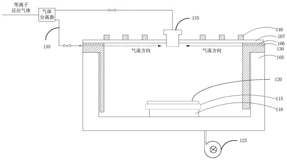
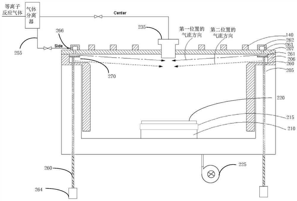
[0043] The following will clearly and completely describe the technical solutions in the embodiments of the present invention with reference to the accompanying drawings in the embodiments of the present invention. Obviously, the described embodiments are only some, not all, embodiments of the present invention. Based on the embodiments of the present invention, all other embodiments obtained by persons of ordinary skill in the art without making creative efforts belong to the protection scope of the present invention.

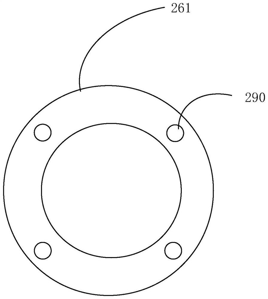
[0044] The following will be combined as figure 2 Shown is a detailed description of one embodiment of the invention. figure 2 A plasma reaction device according to an embodiment of the present invention is shown. In addition to the 2XX series reference designators, figure 2 shown in the corresponding figure 1 The elements in all have the same reference numerals, it should be understood that the plasma reaction device therein is only exemplary, and the p...


PUM


Abstract

The invention provides a plasma reaction device. The plasma reaction device comprises a reaction cavity defined by a shell, a top plate and a lining. A first annular groove is formed in the top of theinner wall of the lining of the plasma reaction device, the side wall and the bottom surface of the first annular groove are arranged on the lining, and the top of the first annular groove is sealedby a top plate; and an airflow channel ring is arranged in the first annular groove, and an edge gas injection channel and / or a reaction gas injector which are / is arranged on the top plate and correspond to the airflow channel ring inject / injects plasma reaction gas into the reaction cavity. A power device connected with the airflow channel ring drives the airflow channel ring to move up and down,the flowing mode of the gas injected into the reaction cavity is changed, diffusion of the injected gas is accelerated, and uniformity of the gas in the reaction cavity is achieved.

Description

technical field [0001] The invention relates to the technical field of semiconductor equipment manufacturing, in particular to the technical field of improving the uniform distribution of plasma. Background technique [0002] Plasma reactors are key equipment for semiconductor chip processing and are widely used to process semiconductor substrates to manufacture integrated circuits. A patterned microelectronic layer is formed on a substrate, and plasma is often used to deposit a thin film on the substrate or etch a predetermined portion of the thin film during substrate processing. The specific method is to first place the substrate fixedly in the plasma reaction chamber; then transmit radio frequency energy into the plasma reaction chamber to form a radio frequency field through the radio frequency power transmitting device; then various reactive gases (etching gas or deposition gas) are injected into the plasma In the reaction chamber, under the action of the radio freque...

Claims


Application Information

Patent Timeline
IPC IPC(8): H01J37/32
CPCH01J37/321H01J37/3244H01J37/32449H01J2237/332H01J2237/334Y02P70/50
Inventor 连增迪左涛涛吴狄
Owner ADVANCED MICRO FAB EQUIP INC CHINA
Why Eureka
Try Eureka