Method for manufacturing a semiconductor device and semiconductor device

A manufacturing method and semiconductor technology, applied in the fields of semiconductor devices, semiconductor/solid-state device manufacturing, electric solid-state devices, etc., can solve the problem of low overcurrent protection capability, and achieve the effect of high current capability and high robustness

Active Publication Date: 2022-06-24
CSMC TECH FAB2 CO LTD
View PDF0 Cites 0 Cited by
  • Summary
  • Abstract
  • Description
  • Claims
  • Application Information

AI Technical Summary

Problems solved by technology

However, in the process of forming the source and drain, in order to prevent the current from concentrating on the surface, the source and drain ion implantation including inclined ion implantation is adopted, and the formed source and drain have a relatively vertical shape under the gate structure to increase the conductivity. area, such as Figure 1B shown, making the current path at the bottom of the source and drain (as Figure 1B Shown in P2) is larger, larger than the current path of the source-drain surface (such as Figure 1B (shown in P1), which makes it easier for the current to concentrate on the surface during electrostatic discharge, and the overcurrent protection capability per unit area is low

Method used


Image

  • Method for manufacturing a semiconductor device and semiconductor device
  • Method for manufacturing a semiconductor device and semiconductor device
  • Method for manufacturing a semiconductor device and semiconductor device

Examples


Embodiment 1

[0030] In order to solve the problems in the prior art, the present invention provides a method for fabricating a semiconductor device and a semiconductor device, including:

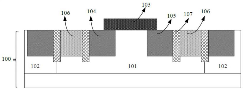
[0031] providing a semiconductor substrate on which a gate structure is formed;

[0032] performing a lightly doped source and drain ion implantation process to form lightly doped source and drain regions in the semiconductor substrate on both sides of the gate structure;

[0033] performing pocket ion implantation to form a pocket ion implantation region at the bottom of the lightly doped source and drain regions;

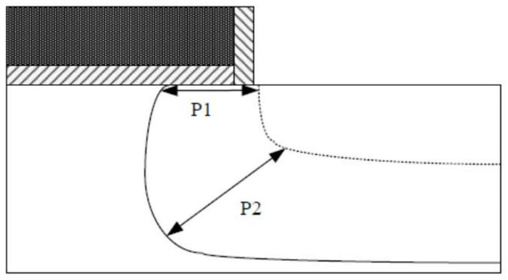
[0034] performing source and drain ion implantation to form source and drain regions in the semiconductor substrate on both sides of the gate, wherein the lightly doped source and drain regions, the pocket ion implantation region and the source and drain regions Together, a source and a drain having an inclined topography under the gate structure are formed.

[0035] Reference below Figu...

Embodiment 2

[0068] The present invention also provides a semiconductor device, manufactured by the method described in Embodiment 1, comprising a semiconductor substrate, a gate structure located on the semiconductor substrate, and the semiconductor device located on both sides of the gate structure. The source and drain in the substrate are composed of lightly doped source and drain regions, pocket-type ion implantation regions and source and drain regions, and have an inclined morphology under the gate structure.

[0069] Exemplarily, the semiconductor substrate is a P-type semiconductor substrate, and the semiconductor device is a GGNMOS device.

[0070] Since the source-drain has a source-drain with a sloped topography under the gate structure, the current path at the bottom of the drain is smaller during the electrostatic discharge, so that more current passes through the bottom of the drain during the electrostatic discharge At this time, the surface current is less likely to be con...


PUM


Abstract

The present invention provides a manufacturing method of a semiconductor device and the semiconductor device. The manufacturing method includes: providing a semiconductor substrate on which a gate structure is formed; performing a lightly doped source-drain ion implantation process to Forming lightly doped source and drain regions in the semiconductor substrate on both sides of the gate structure; performing pocket region ion implantation to form a pocket ion implantation region at the bottom of the lightly doped source and drain region; performing source and drain ion implantation implanted to form source and drain regions in the semiconductor substrate on both sides of the gate, wherein the lightly doped source and drain regions, the pocket ion implantation region and the source and drain regions are jointly formed in the There are source and drain electrodes with inclined topography under the gate structure. According to the manufacturing method of the semiconductor device and the same area of ​​the semiconductor device, it can have a higher current capability (current capability of the transmission line pulse test), so it has higher robustness than conventional technology.

Description

technical field [0001] The present invention relates to the field of semiconductor manufacturing, in particular to a manufacturing method of a semiconductor device and a semiconductor device. Background technique [0002] GGNMOS (Gate Grounded NMOS) is a commonly used ESD protection device. A typical GGNMOS device is shown in FIG. 1 , which includes a semiconductor substrate 100 in which a P well 101 and an N well 102 are formed, wherein the GGNMOS device is formed in the P In the well 101, a gate structure 103 is formed on the semiconductor substrate 100, and a source electrode 104 and a drain electrode 105 are also formed in the semiconductor substrate 100 on both sides of the gate structure 103, wherein the gate structure 103 and the source electrode 104 are formed Together with the lead terminal 106 of the substrate, the anode of the GGNMOS device is formed, the drain 105 is separately led out as a cathode, and an isolation structure 107 is respectively provided between ...

Claims


Application Information

Patent Timeline
Patent Type & Authority Patents(China)
IPC IPC(8): H01L29/78H01L29/08H01L21/336H01L21/265
CPCH01L29/7834H01L29/0847H01L29/66477H01L29/66522H01L29/66068H01L21/26513H01L21/26546H01L21/046H01L29/78H01L29/08H01L21/265H01L27/02
Inventor 梁旦业汪广羊
Owner CSMC TECH FAB2 CO LTD
Why Eureka
Try Eureka