Multilayer thick-film ceramic-based circuit board and preparation process thereof

A preparation process and ceramic substrate technology, which is applied in the direction of printed circuit manufacturing, printed circuit, circuit heating device, etc., can solve the problem that the heat conduction effect of ceramic substrate is not particularly ideal, so as to avoid mechanical or laser drilling, facilitate heat dissipation, and improve quality effect

Active Publication Date: 2021-08-06
SICHUAN RUIHONG ELECTRONIC TECH CO LTD
View PDF19 Cites 0 Cited by
  • Summary
  • Abstract
  • Description
  • Claims
  • Application Information

AI Technical Summary

Problems solved by technology

[0006] However, the heat conduction effect of ordinary ceramic base is still not

Method used


Image

  • Multilayer thick-film ceramic-based circuit board and preparation process thereof
  • Multilayer thick-film ceramic-based circuit board and preparation process thereof
  • Multilayer thick-film ceramic-based circuit board and preparation process thereof

Examples


Embodiment Construction

[0035] The present invention will be further described below in conjunction with the accompanying drawings, but the protection scope of the present invention is not limited to the following description.

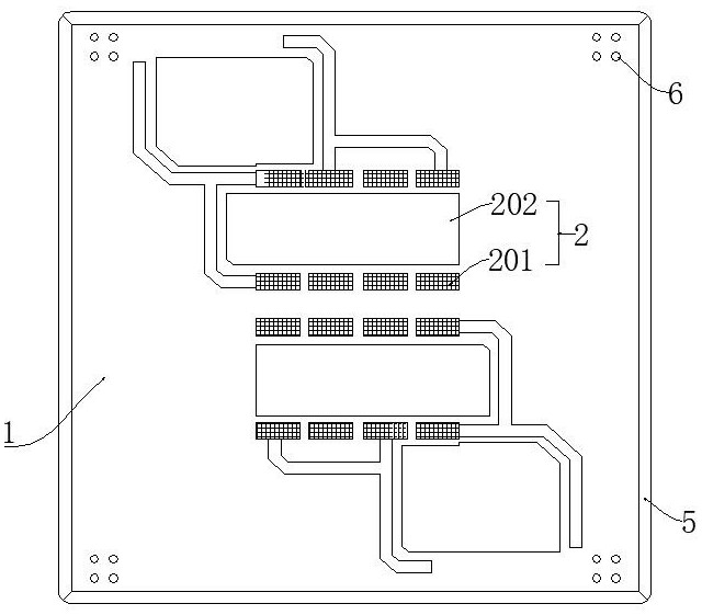
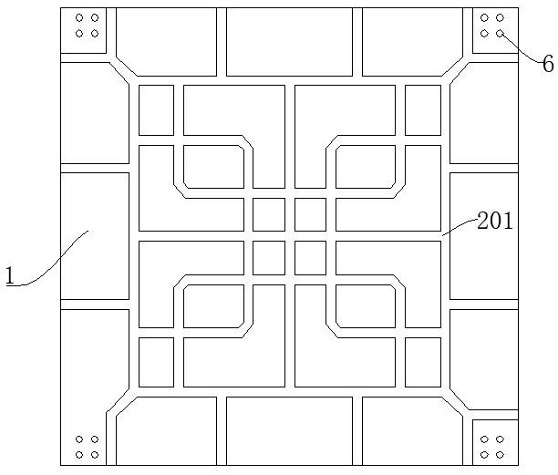
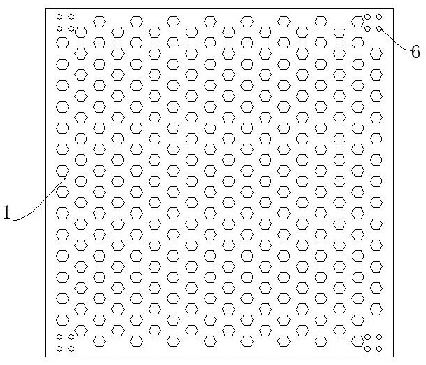
[0036] like Figure 1~Figure 4 As shown, this solution discloses a ceramic substrate 1 , a copper clad layer 2 , and a cladding layer that are laminated sequentially from bottom to top by a multilayer thick-film ceramic-based circuit board.

[0037] In this solution, the ceramic substrate 1 includes a ceramic plate A3 and a ceramic plate B4, the ceramic plate A3 is in the shape of a grid, the ceramic plate B4 is in the shape of a whole plate, and two ceramic plates B4 clamp and bond the ceramic plate A3. In this way, heat dissipation holes are formed between the mesh holes.

[0038] In this solution, the copper clad layer 2 is bonded to the surface of the ceramic board B4, after which a printed circuit line 201 and a heat dissipation copper area 202 are formed. The heat diss...


PUM


Abstract

The invention relates to a multilayer thick-film ceramic-based circuit board. The circuit board comprises a ceramic substrate, a copper-clad layer and a cladding layer which are sequentially laminated from bottom to top; the ceramic substrate comprises a ceramic plate A and ceramic plates B, the ceramic plate A is clamped and bonded by the two ceramic plates B, the ceramic plate A is in a grid shape, and each ceramic plate B is in a whole plate shape; and the copper-clad layer is bonded to the surfaces of the ceramic plates B, a printed circuit line and a heat dissipation copper area are formed after the copper-clad layer is bonded to the surfaces of the ceramic plates B, and the heat dissipation copper area is separated from the printed circuit line and used for dissipating heat. The invention further discloses a preparation process of the circuit board. The heat dissipation effect is good, the strength is high, the preparation is convenient, and the production cost is low.

Description

technical field [0001] The invention relates to the technical field of circuit board preparation, in particular to a multilayer thick-film ceramic-based circuit board and a preparation process thereof. Background technique [0002] When it comes to substrates, they are often thought of as resin-based printing substrates. In recent years, the resin used for printing substrates has also continued to improve. It has been upgraded from traditional low-cost, easy-to-process Phenol resins to better thermal stability. Epoxy glass substrate (Glass Epoxy), polyimide, etc. [0003] However, in the world of information-related products, in order to continuously increase the computing speed, the transistor density of the chip is also increased, because with this, the thermal effect of the chip packaged on the substrate is also increased. Therefore, from the late 1970s, the industry began to find that the resin printed substrates used in high-integration chip packaging gradually experie...

Claims


Application Information

Patent Timeline
IPC IPC(8): H05K1/02H05K3/00H05K3/22
CPCH05K1/02H05K1/0203H05K3/00H05K3/227
Inventor 陈绍智陈雪郑海军熊凌鹏张勇罗伟杰
Owner SICHUAN RUIHONG ELECTRONIC TECH CO LTD
Why Eureka
Try Eureka