MOS device and method for preventing parasitic transistor of MOS device from being turned on

A MOS device, body extraction technology, applied in semiconductor devices, semiconductor/solid-state device manufacturing, electrical components, etc., can solve the problems of increased off-state leakage of MOS devices and reduced electrical characteristics of MOS devices

Active Publication Date: 2021-03-09
INST OF MICROELECTRONICS CHINESE ACAD OF SCI
View PDF7 Cites 0 Cited by
  • Summary
  • Abstract
  • Description
  • Claims
  • Application Information

AI Technical Summary

Problems solved by technology

[0005] Aiming at the problems existing in the prior art, the embodiment of the present invention provides a MOS device and a method for avoiding the turning on of the parasitic transistor of the MOS device, which is used to solve the parasitic transistor effect caused by

Method used


Image

  • MOS device and method for preventing parasitic transistor of MOS device from being turned on
  • MOS device and method for preventing parasitic transistor of MOS device from being turned on
  • MOS device and method for preventing parasitic transistor of MOS device from being turned on

Examples


Embodiment 1

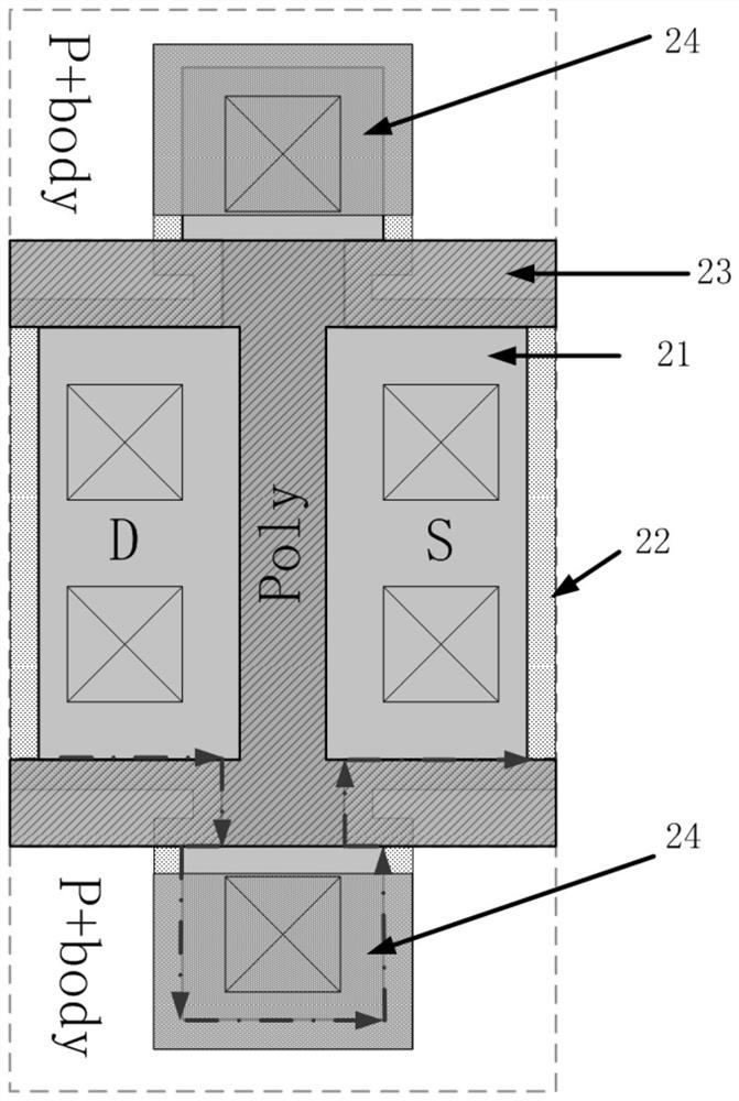
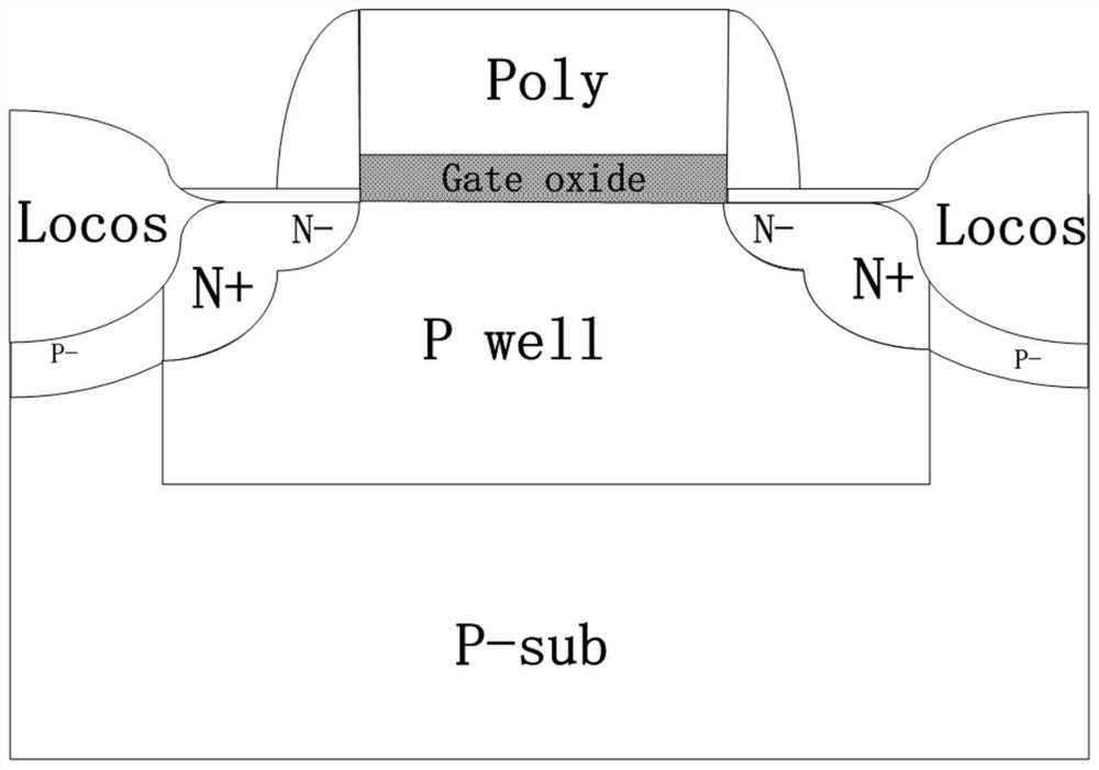
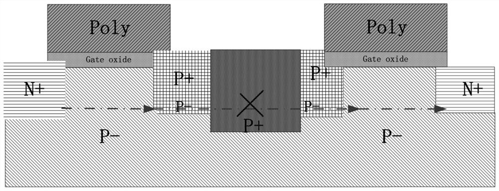
[0039] This embodiment provides a MOS device. The MOS device may include an NMOS device or a PMOS device. When the MOS device is an NMOS device, such as figure 1 and figure 2 As shown, the MOS device includes: a silicon substrate P-sub, a field oxygen region, an active region 21, a well region P well, a body lead-out region P+body, a gate dielectric layer Gate oxide, an H-type gate bar 23 and an active Field injection region 22 at region edge 21 .

[0040] Wherein, the active region 21 includes a source region S, a drain region D and a channel region, and the body lead-out region is arranged on one side in the width direction of the H-shaped gate bar;

[0041] An implantation window is set on the body lead-out region, and the interface region between the back of the field oxygen region and the silicon substrate is a heavily doped region; the doping concentration of the heavily doped region is higher than that of the well region; the secondary ion implantation The depth is g...


PUM


Abstract

The invention provides an MOS device and a method for preventing a parasitic transistor of the MOS device from being turned on. The MOS device comprises a silicon substrate, a field oxide region, an active region, a well region, a body leading-out region, a gate dielectric layer and an H-shaped grid bar which are located above the silicon substrate, and a field injection region located at the edgeof the active region, wherein the active region comprises a source region, a drain region and a channel region, and the body leading-out region is arranged on one side of the H-shaped grid bar in thewidth direction; an injection window is arranged on the body leading-out region, and an interface region between the back surface of the field oxygen region and the silicon substrate is a heavily doped region; the doping concentration of the heavily doped region is higher than that of the well region; and the depth of the secondary ion injection is greater than or equal to the ion injection depths of the source region and the drain region. Therefore, the window is additionally arranged above the body leading-out region, secondary ion injection is carried out along the injection window, it isensured that the edge of the field oxide region has enough high doping concentration, the parasitic transistor cannot be turned on, off-state electric leakage of the MOS device is inhibited, and the electrical characteristics of the MOS device are improved.

Description

technical field [0001] The invention belongs to the technical field of semiconductor devices, in particular to a MOS device and a method for preventing parasitic transistors from being turned on in the MOS device. Background technique [0002] CMOS integrated circuits have many advantages such as low power consumption, fast speed, strong anti-interference ability, and high integration. Therefore, CMOS technology is the mainstream technology of large-scale integrated circuits. [0003] Whether it is based on bulk silicon or SOI substrate materials, the leakage of MOS devices themselves and each other has always been an urgent problem to be solved in the industry. Therefore, the isolation technology of MOS devices is a key technology in the integrated circuit manufacturing process. Cause leakage, breakdown, latch-up effect, etc. [0004] In the prior art, commonly used isolation process technologies include junction isolation, Local Oxidation of Silicon (LOCOS, Local Oxidatio...

Claims


Application Information

Patent Timeline
IPC IPC(8): H01L29/78H01L29/06H01L29/36H01L21/336
CPCH01L29/78H01L29/0607H01L29/0684H01L29/36H01L29/66477
Inventor 高林春曾传滨李晓静闫薇薇李多力单梁钱频张颢译倪涛罗家俊韩郑生
Owner INST OF MICROELECTRONICS CHINESE ACAD OF SCI
Why Eureka
Try Eureka