Method for eliminating solder mask ink in via hole of printed circuit board
What is Al technical title?
Al technical title is built by PatSnap Al team. It summarizes the technical point description of the patent document.
A technology for printed circuit boards and solder mask inks, which is applied in the directions of printed circuits, printed circuit manufacturing, and printed circuit secondary processing. Difficulty, improve cleaning effect, reduce production cost effect
Active Publication Date: 2021-03-12
四川英创力电子科技股份有限公司
View PDF9 Cites 2 Cited by
Summary
Abstract
Description
Claims
Application Information
AI Technical Summary
This helps you quickly interpret patents by identifying the three key elements:
Problems solved by technology
Method used
Benefits of technology
Problems solved by technology
[0002] In the production process of printed circuit boards, the ink will block the small-diameter via holes when printing with solder resist ink, and when the customer requires that there should be no residual ink in the via holes, the existing method is to print the screen on the screen. A baffle or a plug is set on the position corresponding to the via hole, but the production of the printing screen in this way is difficult and costly, and the position accuracy of the plug behind the baffle is not easy to control, and it is impossible to completely and effectively avoid the solder resist ink. Into the via hole, and this method can only be printed on one side, and when making a double-sided circuit board, it is necessary to print on both sides separately, and the production efficiency is low
Another method is to perform back development on the defective products with solder resist ink entering the via holes, and this method will lead to excessive development during the second development, showing such Figure 7 The state shown leads to the lack of ink at the edge of the via hole, and even the occurrence of undesirable phenomena such as the isolation of solder bridges between ICs, resulting in rework or scrapping of the circuit board
Method used
Image
Click on the blue label to locate the original text in one second.
Reading with bidirectional positioning of images and text.
Examples
Embodiment
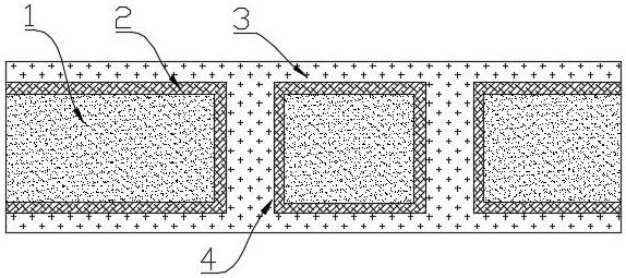
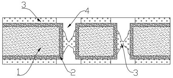
[0045] Such as figure 1 As shown, a method for eliminating the solder resist ink in the via hole of a printed circuit board, the method of the present invention is applicable to circuit boards whose via hole 4 has an aperture diameter of 0.2mm to 0.5mm, such as 0.2mm, 0.25mm, 0.3 mm, 0.35mm, 0.45mm, 0.5mm are all available.
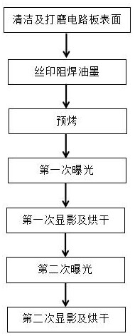
[0046] This embodiment takes a double-sided circuit board as an example, and the method includes the following steps:
[0047] S1: clean the substrate 1 and the conductive copper layer 2 on the surface of the substrate 1, roughen the surface of the conductive copper layer 2 with a polishing device 10, improve the bonding of the solder resist ink, and clean the substrate 1 and the conductive copper layer 2 again, The two cleanings are carried out by water washing or ultrasonic to remove dust and impurities on the surface of the circuit board.
[0048] S2: silk screen printing, on the conductive copper layer 2, print the ink layer 3 of the predetermined co...
PUM
Property
Measurement
Unit
pore size
aaaaa
aaaaa
Abstract
The invention discloses a method for eliminating solder mask ink in a via hole of a printed circuit board, which comprises the steps of S1, cleaning a substrate and a conductive copper layer on the surface of the substrate, roughening the surface of the conductive copper layer through a polishing device, and cleaning the substrate and the conductive copper layer again; S2, carrying out silk-screenprinting, specifically, printing an ink layer with a preset color on the conductive copper layer; S3, conducting pre-baking, specifically, pre-baking the silk-screen printed circuit board; S4, performing primary exposure, specifically, performing alignment exposure by using a film, performing photocuring on the solder mask ink, and shielding the via hole and the periphery by using a shading partof the film; S5, developing for the first time, and removing the ink at the position shielded by the shading part of the film; S6, drying the circuit board. S7, performing secondary exposure, specifically, performing secondary alignment exposure by using a film, and performing secondary photocuring on the ink layer; S8, developing for the second time, and removing the residual solder resist ink inthe via hole; and S9, drying the circuit board. The solder mask ink in the via hole can be effectively eliminated, the integrity of an ink layer is ensured, and assembly welding bridge partition is prevented.
Description
technical field [0001] The invention belongs to the field of circuit board production, in particular to a method for eliminating solder resist ink in a through hole of a printed circuit board. Background technique [0002] In the production process of printed circuit boards, the ink will block the small-diameter via holes when printing with solder resist ink, and when the customer requires that there should be no residual ink in the via holes, the existing method is to print the screen on the screen. A baffle or a plug is set on the position corresponding to the via hole, but the production of the printing screen in this way is difficult and costly, and the position accuracy of the plug behind the baffle is not easy to control, and it is impossible to completely and effectively avoid the solder resist ink. Into the via hole, and this method can only be used for single-sided printing, and when making a double-sided circuit board, it is necessary to print on both sides separat...
Claims
Application Information
Patent Timeline
Application Date:The date an application was filed.
Publication Date:The date a patent or application was officially published.
First Publication Date:The earliest publication date of a patent with the same application number.
Issue Date:Publication date of the patent grant document.
PCT Entry Date:The Entry date of PCT National Phase.
Estimated Expiry Date:The statutory expiry date of a patent right according to the Patent Law, and it is the longest term of protection that the patent right can achieve without the termination of the patent right due to other reasons(Term extension factor has been taken into account ).
Invalid Date:Actual expiry date is based on effective date or publication date of legal transaction data of invalid patent.