Lateral double-diffused metal oxide semiconductor device and manufacturing method thereof, and electronic device

A technology of oxide semiconductor and lateral double diffusion, which is applied in semiconductor/solid-state device manufacturing, semiconductor devices, circuits, etc.

Active Publication Date: 2021-03-19
CSMC TECH FAB2 CO LTD
View PDF20 Cites 1 Cited by
  • Summary
  • Abstract
  • Description
  • Claims
  • Application Information

AI Technical Summary

Problems solved by technology

However, so far, SJ technology has only been maturely applied in vertical discrete transistors (vertical discrete transistors), such as VDMOS or IGBT

Method used


Image

  • Lateral double-diffused metal oxide semiconductor device and manufacturing method thereof, and electronic device
  • Lateral double-diffused metal oxide semiconductor device and manufacturing method thereof, and electronic device
  • Lateral double-diffused metal oxide semiconductor device and manufacturing method thereof, and electronic device

Examples


Embodiment Construction

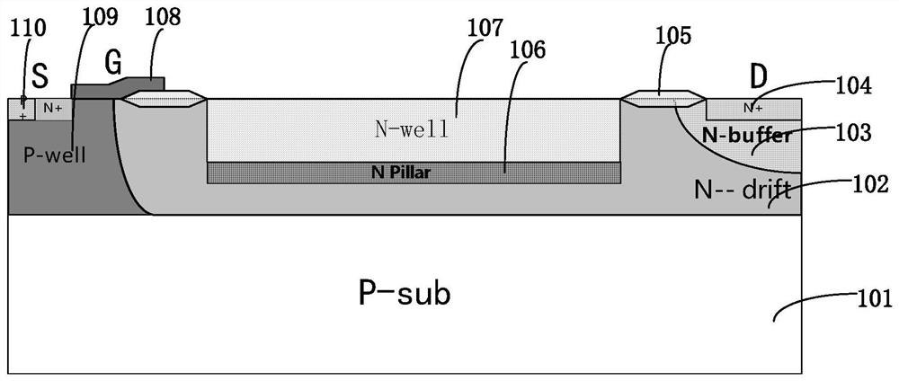
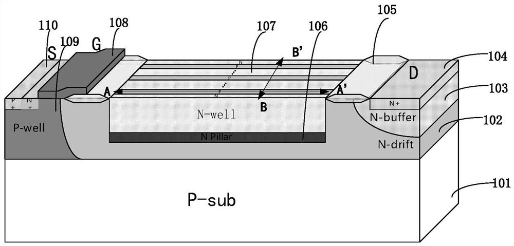
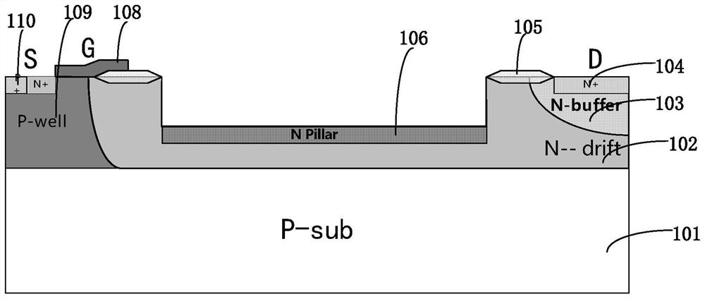
[0040] In the following description, numerous specific details are given in order to provide a more thorough understanding of the present invention. It will be apparent, however, to one skilled in the art that the present invention may be practiced without one or more of these details. In other examples, some technical features known in the art are not described in order to avoid confusion with the present invention.

[0041] It should be understood that the invention can be embodied in different forms and should not be construed as limited to the embodiments set forth herein. Rather, these embodiments are provided so that this disclosure will be thorough and complete, and will fully convey the scope of the invention to those skilled in the art. In the drawings, the size and relative sizes of layers and regions may be exaggerated for clarity, and like reference numerals designate like elements throughout.

[0042] It will be understood that when an element or layer is referr...


PUM

PropertyMeasurementUnit
thicknessaaaaaaaaaa

Abstract

The invention provides a lateral double-diffused metal oxide semiconductor device and a manufacturing method thereof, and an electronic device. The method comprises the following steps: providing a semiconductor substrate, and forming a drift region in the semiconductor substrate; forming a well region and a drain region in the drift region, and forming a source region and a channel in the well region; executing ion implantation of a first type so as to form a first ion implantation region extending along a direction from well region to drain region at the bottom of the drift region; forming aplurality of mutually spaced deep trench isolation structures above the first ion implantation region and fin structures located between adjacent deep trench isolation structures; forming a second ion implantation region so as to allow the first ion implantation region and the second ion implantation region to be alternately arranged; and performing ion implantation of a second type on the side walls of the fin structures to form side wall ion implantation regions on the side walls of the fin structures, wherein the ions of the first type are different from the ions of the second type.

Description

technical field [0001] The invention relates to the technical field of semiconductors, in particular to a lateral double-diffused metal oxide semiconductor device, a manufacturing method, and an electronic device. Background technique [0002] In the development of high-voltage MOS transistors, there are mainly two types: vertical double-diffused metal-oxide semiconductor (VDMOS) and lateral double-diffused metal-oxide semiconductor (LDMOS). Although vertical double-diffused metal-oxide semiconductor (VDMOS) has a small on-resistance and occupies a small layout area, it is a vertical structure and is not easy to be compatible with low-voltage CMOS circuits. The lateral double diffused metal oxide semiconductor (LDMOS) has better thermal stability and frequency stability, higher gain and durability, lower feedback capacitance and thermal resistance, and constant input impedance and simpler bias current Circuits, therefore, have been widely used at present. [0003] In the c...

Claims


Application Information

Patent Timeline
Patent Type & Authority Applications(China)
IPC IPC(8): H01L21/336H01L29/06H01L29/78
CPCH01L29/66681H01L29/7816H01L29/7824H01L29/0684H01L21/762H01L29/7835H01L29/0634H01L29/66659H01L29/42368H01L29/0847H01L29/66636H01L29/0653H01L29/7834H01L21/26586H01L21/266
Inventor 何乃龙
Owner CSMC TECH FAB2 CO LTD
Why Eureka
Try Eureka