Quantum interference detection chip and test system thereof

A quantum interference and single-photon detector technology, applied in the field of integrated quantum optics, can solve problems such as the difficulty of large-scale expansion of quantum optical paths, and achieve the effect of meeting the trend of on-chip integration

Active Publication Date: 2021-03-23
SHANGHAI INST OF MICROSYSTEM & INFORMATION TECH CHINESE ACAD OF SCI
View PDF8 Cites 1 Cited by
  • Summary
  • Abstract
  • Description
  • Claims
  • Application Information

AI Technical Summary

Problems solved by technology

However, the current integrated quantum optical circuit is mainly a quantum network composed of waveguide interferometers that encode information in the path, and this quantum optical circuit cannot be easily expanded on a large scale.

Method used


Image

  • Quantum interference detection chip and test system thereof
  • Quantum interference detection chip and test system thereof

Examples


Embodiment Construction

[0015]The present invention is further illustrated in connection with the specific embodiments. It will be appreciated that these examples are intended to illustrate the invention and are not intended to limit the scope of the invention. It will be appreciated that after reading the contents of the present invention, those skilled in the art can make various modifications or modifications to the present invention, and these equivalents also fall in the scope of the claims appended claims.

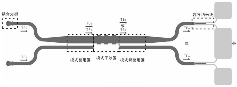
[0016]Embodiments of the invention relate to a quantum interference detection chip, such asfigure 1 As shown, including a coupling grating sequentially connected, an input orientation coupler, a grating mode beam splitter, an output directional coupler, and a superconducting noodle single photon detector, the coupling grating is used to convert the sheet from spontaneous parameters. The entangled photon inputs two input ports of the orientation coupler on each coupled feed; the input directional cou...


PUM


Abstract

The invention relates to a quantum interference detection chip, which comprises a coupling grating, an input directional coupler, a grating mode beam splitter, an output directional coupler and a superconducting nanowire single-photon detector. The coupling grating is used for respectively coupling an entangled photon pair generated by off-chip spontaneous parametric down-conversion into two inputports of the on-chip input directional coupler; the input directional coupler is used for converting the input entangled photon pair into a transverse electric fundamental mode photon and a transverse electric second-order mode photon; the grating mode beam splitter has a light splitting characteristic on incident transverse electric fundamental mode light and transverse electric second-order mode light, so that two-photon interference in mode is realized; the output directional coupler is used for transmitting a pair of photons which are simultaneously in a transverse electric fundamental mode or a transverse electric second-order mode and are subjected to mode interference to a certain output port; and the superconducting nanowire single-photon detector absorbs a pair of photons at a low temperature and converts the photons into current signals to be detected by peripheral test equipment. According to the invention, the density of an integrated quantum optical path can be improved.

Description

Technical field[0001]The present invention relates to the field of integrated quantum optical technology, and more particularly to a quantum interference detection chip and a test system thereof.Background technique[0002]The development of integrated quantum optics reduces the quantum optical experiment platform of free space to the chip scale, providing possibilities for demonstrating large-scale quantum calculations. However, the current integrated quantum optical path is mainly a quantum network constructed by a waveguide interferometer of path encoding information, and such a quantum optical path is difficult to easily expand by large scale. In order to achieve scalability in order to simplify quantum calculation architecture or improve quantum communication channel security and anti-noise ability, the operating dimension of the current quantum optical system can be appropriately added, and multiple degrees of freedom, such as light. Waveguide mode, polarization, time, frequency...

Claims


Application Information

Patent Timeline
Patent Type & Authority Applications(China)
IPC IPC(8): G01J11/00G01M11/02G01R31/28
CPCG01J11/00G01M11/02G01R31/2851
Inventor 陶略李杨甘甫烷
Owner SHANGHAI INST OF MICROSYSTEM & INFORMATION TECH CHINESE ACAD OF SCI
Why Eureka
Try Eureka