Check patentability & draft patents in minutes with Patsnap Eureka AI!

Circuit structure and method for preventing I2C interface from mistakenly waking up SOC system

A technology with circuit structure and interface errors, applied in the direction of electrical digital data processing, instruments, etc., can solve the problem of chip wake-up error, waste of energy and other problems

Pending Publication Date: 2021-03-23
BEIJING CEC HUADA ELECTRONIC DESIGN CO LTD
View PDF3 Cites 3 Cited by
  • Summary
  • Abstract
  • Description
  • Claims
  • Application Information

AI Technical Summary

Problems solved by technology

[0003] In the existing low-power design, when the chip is in a low-power state, due to the harsh working environment, the glitch signal of the chip interface will cause the chip to be woken up by mistake and exit the low-power mode until the next work. A lot of energy is wasted during this

Method used


Image

  • Circuit structure and method for preventing I2C interface from mistakenly waking up SOC system
  • Circuit structure and method for preventing I2C interface from mistakenly waking up SOC system

Examples


Embodiment Construction

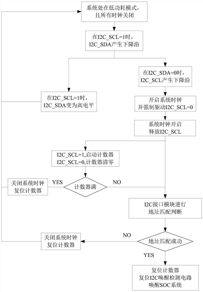
[0025] combine figure 1 , a schematic diagram of the circuit structure of the present invention, illustrating the circuit structure of the present invention.

[0026] The I2C bus signal (101) conforms to the standard I2C bus protocol, and is directly connected to the interface of the host.

[0027] Glitch filtering circuit (108), including I2C_SDA falling edge detection register (102), I2C_SDA rising edge detection register (103) and I2C_SCL falling edge detection register (104), respectively detects the rising edge of I2C_SDA, I2C_SDA falling edge and I2C_SCL falling edge.

[0028] The output end of the above-mentioned I2C_SDA falling edge detection register (102) is respectively connected to the reset end of the I2C_SCL falling edge detection register (104) and the reset end of the rising edge detection register (103) of I2C_SDA.

[0029] The output of the rising edge detection register (103) of I2C_SDA is connected to the reset terminal of the I2C_SCL falling edge detecti...


PUM


Abstract

The invention belongs to the field of SOC system low-power-consumption design. The invention discloses a circuit structure and method for preventing an SOC system from being mistakenly awakened by I2Cinterface burrs. The invention provides a circuit capable of filtering and detecting burrs of an I2C bus signal (101) in order to overcome the defect that the SOC is awakened by an I2C interface mistakenly due to the burrs of the I2C bus signal (101) when the SOC is in a complex working environment. According to the circuit, the burr filtering circuit (108) is used for respectively detecting therising edge and the falling edge of the I2CSDA bus and the falling edge of the I2CSCL bus, so that burrs on the I2CSCL bus or the I2CSDA bus can be effectively filtered. When an I2C start timing is detected, the system clock turn-on circuit (106) operates to turn on the system clock. And in the process of detecting whether the address is matched (107) by the I2C interface, when the counter (105) counts to a set value and the address matching is still not finished, indicating that the initial time sequence is caused by burrs generated by the I2CSCL and the I2CSDA at the same time, closing the system clock, resetting the counter and recovering the SOC to a low-power-consumption mode.

Description

technical field [0001] The invention belongs to the field of SOC system low power consumption design. A circuit structure and method to prevent the I2C interface from waking up the SOC system by mistake are proposed. Background technique [0002] With the gradual increase in the scale of SOC chips, the power consumption of the chip has become the main indicator for evaluating the performance of a chip, and low power consumption is also one of the most competitive features of the chip. How to reduce the power consumption of the chip and ensure that the chip is kept in a low power consumption state as much as possible in the idle state are two directions that SOC chip design is constantly pursuing. [0003] In the existing low-power design, when the chip is in a low-power state, due to the harsh working environment, the glitch signal of the chip interface will cause the chip to be woken up by mistake and exit the low-power mode until the next work. A lot of energy is wasted ...

Claims


Application Information

Patent Timeline
Patent Type & Authority Applications(China)
IPC IPC(8): G06F13/42
CPCG06F13/4282Y02D10/00
Inventor 梁瀚予崔浩林
Owner BEIJING CEC HUADA ELECTRONIC DESIGN CO LTD
Features
  • R&D
  • Intellectual Property
  • Life Sciences
  • Materials
  • Tech Scout
  • Unparalleled Data Quality
  • Higher Quality Content
  • 60% Fewer Hallucinations
Learn More