
A method of fabricating super junction mosfet with enhanced uis capability

A manufacturing method and capability technology, applied in the field of super-junction MOSFET manufacturing to improve UIS capability, can solve problems such as smaller injection window, unsatisfactory P+deepbody area, and limited super-junction MOSFET UIS capability

Active Publication Date: 2021-06-04
SEMICON MFG ELECTRONICS (SHAOXING) CORP +1
View PDF4 Cites 0 Cited by
  • Summary
  • Abstract
  • Description
  • Claims
  • Application Information

AI Technical Summary

Problems solved by technology

[0005] When reducing the resistance of the base region, increasing the doping concentration and area of ​​the P+ deep body region is an effective method, but usually the formation of the P+ deep body region is to form an isolation spacer on the side wall of the gate (usually the isolation side wall is referred to as Spacer) Afterwards, due to the existence of the Spacer, the injection window becomes smaller, and the lateral expansion of the P+ deepbody region is limited under the influence of the Spacer's lateral size, so the area of ​​the P+ deep body region cannot reach the ideal state, which limits the UIS of the super-junction MOSFET. ability

Method used


Image

  • A method of fabricating super junction mosfet with enhanced uis capability
  • A method of fabricating super junction mosfet with enhanced uis capability
  • A method of fabricating super junction mosfet with enhanced uis capability

Examples


Embodiment Construction

[0028] The technical solutions in the embodiments of the present invention will be clearly and completely described below in conjunction with the drawings in the embodiments of the present invention.

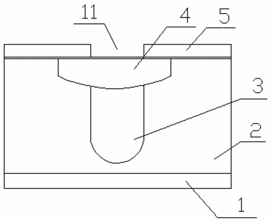
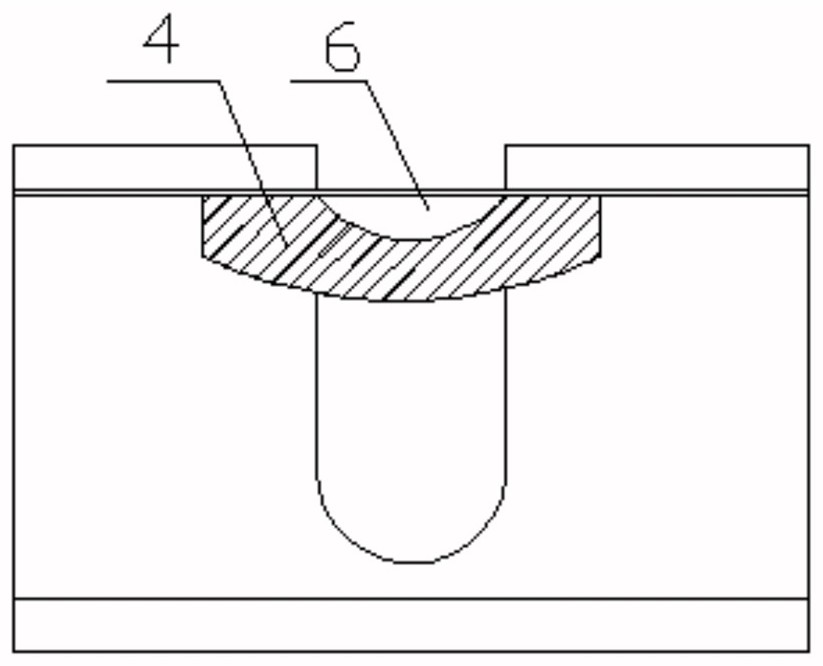
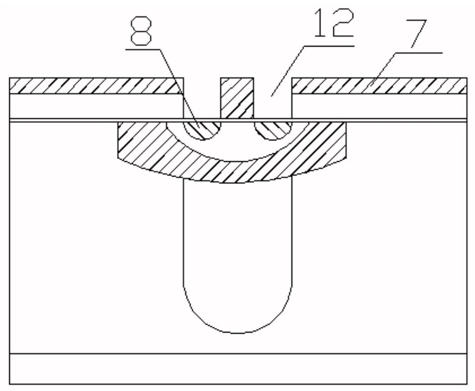
[0029] This embodiment discloses a method for manufacturing a super-junction MOSFET with improved UIS capability, in which part of the content of this embodiment is omitted for the conventional process steps of manufacturing a super-junction MOSFET in the prior art, and this embodiment only focuses on the process related to the purpose of the invention The key points of the link are explained. The super-junction MOSFET mentioned in this embodiment is an example of a planar gate deep-trench super-junction MOSFET, and its manufacturing process is as follows: Figure 5 As shown, the device structure formed at different stages in the fabrication process exhibits the Figure 1 to Figure 4 shown.

[0030] First select the semiconductor substrate 1, and then form an epitaxial layer 2...


PUM


Abstract

The invention relates to a method for manufacturing a superjunction MOSFET with improved UIS capability. The method first forms a P-type column and a P-type body region on the epitaxial layer of the substrate, and implants high-dose P from the implantation window before forming the source region. Type impurity but no annealing operation, and then inject N type impurity according to the existing process method to form the source region; since the injection window is not laterally blocked by the isolation side wall before the source region is formed, it is conducive to the lateral diffusion of the high dose implanted P type impurity, The second implanted P-type impurity is pushed to the depth direction by means of the annealing operation during the formation of the source region, which increases the area distribution of the high-concentration P-type impurity, which is beneficial to reduce the base resistance of the BJT; in the source region and gate After the isolation sidewall of the pole sidewall is formed, a high dose of P-type impurity is implanted for the third time and annealed. The second and third implantation of P-type impurity increases the doping concentration of the base region, and can also make the base region The resistance is significantly reduced to achieve the purpose of improving the UIS capability of the device.

Description

technical field [0001] The invention relates to the technical field of semiconductors, in particular to a method for manufacturing a super-junction MOSFET with improved UIS capability. Background technique [0002] UIS (Unclamped Inductive Switching) is the "unclamped inductive load switching process". UIS capability is an important indicator to measure the reliability of power devices. For power devices, it is required to have high avalanche tolerance in UIS, that is, to have high anti-UIS avalanche breakdown capability. This is because the energy stored in the inductive load under UIS conditions requires all power MOS transistors to be turned off. Release, when the high current stress in the circuit can easily lead to device failure. [0003] Studies have shown that there is a natural parasitic transistor (BJT) in the MOSFET body. Taking N-type MOSFET as an example, the N-type epitaxial layer, P+ active region and N+ active region constitute an NPN-type triode, which is l...

Claims


Application Information

Patent Timeline
Patent Type & Authority Patents(China)
IPC IPC(8): H01L21/336H01L21/265H01L29/78H01L29/06
CPCH01L21/26513H01L29/0634H01L29/66712H01L29/7802
Inventor 秦芳莉韩廷瑜何云梁路陈会治罗顶
Owner SEMICON MFG ELECTRONICS (SHAOXING) CORP
Learn More