A Semi-Superjunction MOSFET with Auxiliary Buried Oxide

A buried oxide and semi-superjunction technology, which is applied in semiconductor devices, semiconductor/solid-state device manufacturing, electrical components, etc., can solve the problem of increasing the threshold voltage of MOSFET devices, preventing the parasitic BJT tube from being turned on completely, and reducing the parasitic BJT base area Resistance and other issues, to improve the UIS capability, increase the contribution, and avoid the effect of opening

Active Publication Date: 2020-05-01
UNIV OF ELECTRONICS SCI & TECH OF CHINA
View PDF4 Cites 0 Cited by
  • Summary
  • Abstract
  • Description
  • Claims
  • Application Information

AI Technical Summary

Problems solved by technology

Such a solution still cannot completely eliminate the turn-on of the parasitic BJT tube, and it cannot completely avoid the device failure problem caused by avalanche breakdown; in addition, it cannot reduce the N+ of the power MOSFET through high-energy boron implantation or deep diffusion. The resistance of the P-body region under the source region can infinitely reduce the resistance of the parasitic BJT base region, because this will increase the threshold voltage (channel turn-on voltage) of the MOSFET device

Method used


Image

  • A Semi-Superjunction MOSFET with Auxiliary Buried Oxide
  • A Semi-Superjunction MOSFET with Auxiliary Buried Oxide
  • A Semi-Superjunction MOSFET with Auxiliary Buried Oxide

Examples


Embodiment 1

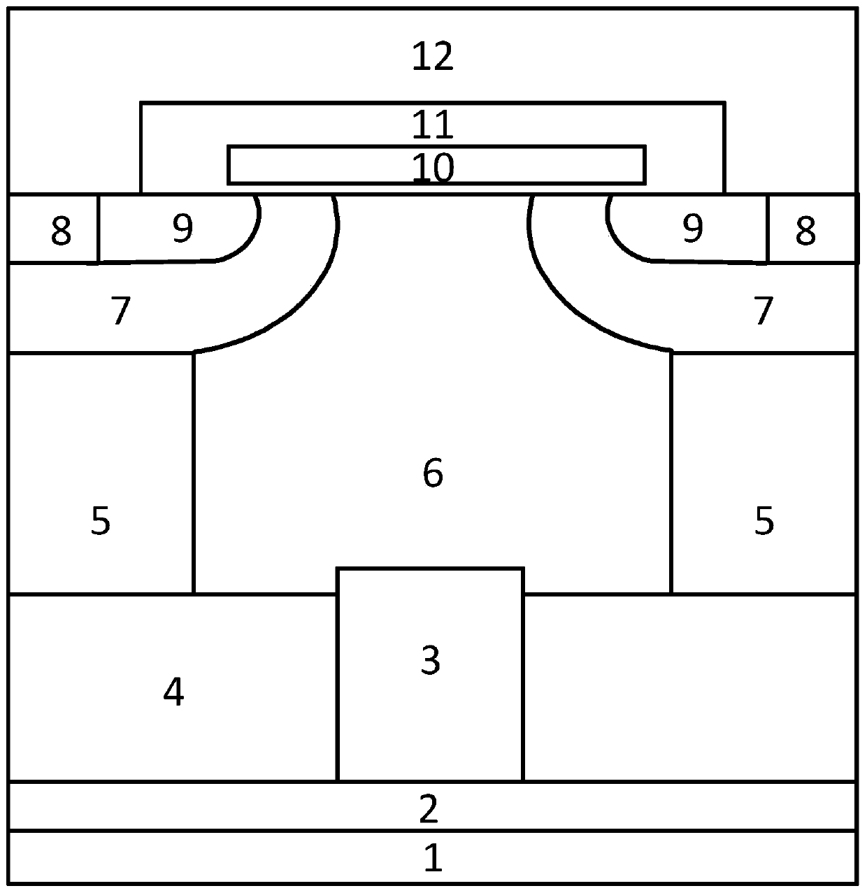
[0021] A semi-superjunction MOSFET with assisted buried oxide, such as figure 1As shown, it includes metallized drain electrode 1, first conductivity type semiconductor highly doped substrate 2, first conductivity type semiconductor doped bottom auxiliary layer 4, second conductivity type semiconductor doped column region 5, first conductivity type semiconductor Doped column region 6, polysilicon gate electrode 10, gate dielectric layer 11 and metallized source electrode 12; the first conductive type semiconductor doped substrate 2 is arranged on the upper end surface of the metallized drain electrode 1; the first conductive Type semiconductor doped bottom auxiliary layer 4 is arranged on the upper end surface of the first conductivity type semiconductor doped substrate 2; the second conductivity type semiconductor doped column region 5 and the first conductivity type semiconductor doped column region 6 are arranged on the first conductivity type semiconductor doped column reg...

Embodiment 2

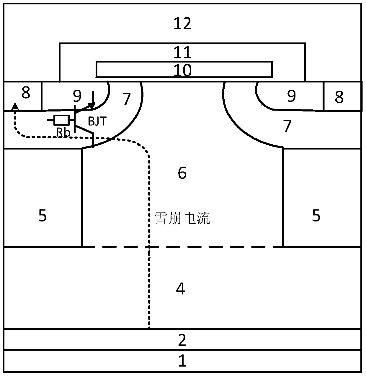
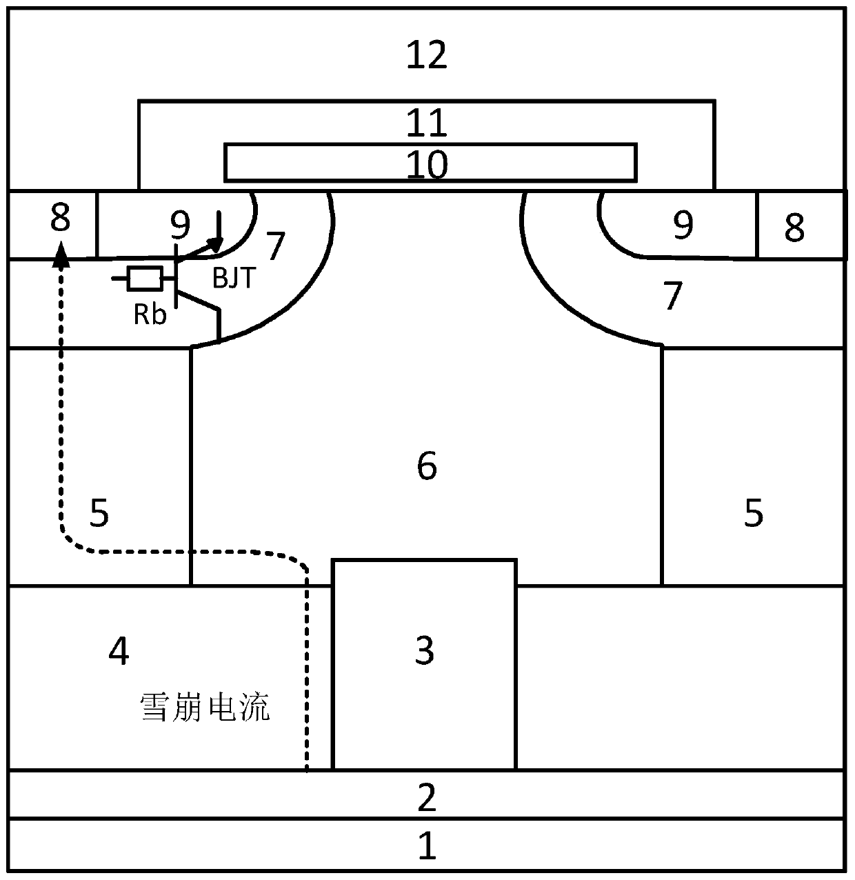
[0030] Such as Figure 7 As shown, the structure of this example is based on Example 1, and the two ends of the metallized source electrode 12 described in Example 1 are extended downwards into the semiconductor body region 7 of the second conductivity type to form a trench structure; The second conductive type semiconductor doped contact region 8 is located at the bottom of the trench with the metallized source electrode 12 at both ends. The structure can further optimize the avalanche current path and improve the UIS capability of the device.

[0031] In the above embodiments, silicon carbide, gallium arsenide, silicon germanium and other semiconductor materials can also be used instead of silicon when making devices.


PUM


Abstract

The invention provides a semi-superjunction MOSFET with an auxiliary buried oxide layer. The auxiliary buried oxide layer is introduced into the auxiliary layer doped with the bottom of the semiconductor of the first conductivity type, and the upper surface of the buried oxide layer is higher than that of the semiconductor of the first conductivity type. The upper end surface of the doped bottom auxiliary layer is located in the doped column region of the first conductivity type semiconductor, and the introduced auxiliary buried oxide layer changes the electric field distribution in the first conductivity type doped bottom auxiliary layer region, increasing its impact on the withstand voltage , thereby increasing the withstand voltage of the device, and at the same time assisting the buried oxide layer, the electric field peak is introduced near the bottom of the semiconductor doped column region of the second conductivity type of the semi-superjunction MOSFET, thereby fixing the avalanche breakdown point at the second conductivity Type semiconductor doping near the bottom of the column area finally makes the avalanche breakdown current path avoid the base resistance of the parasitic BJT, and effectively avoids the opening of the parasitic triode when the semi-superjunction MOSFET device has an avalanche breakdown, thereby improving the performance of the semi-superjunction MOSFET. device reliability in unclamped inductive load applications.

Description

technical field [0001] The invention belongs to the technical field of semiconductor power devices, and relates to a semi-superjunction MOSFET with an auxiliary buried oxide layer. Background technique [0002] Super Junction (Super Junction, abbreviated as SJ) MOSFET breaks the "silicon limit" of conventional power MOSFETs, and has the characteristics of small on-resistance and low switching loss. [0003] However, super-junction MOSFETs also have some disadvantages. First of all, from the perspective of technology, in order to prepare MOSFETs, epitaxial growth and ion implantation are required alternately. The cost required to prepare super-junction MOSFETs is proportional to the number of epitaxial growths. If buried trench With the method of epitaxial growth, the difficulty of the process also increases with the increase of the ratio of the depth and width of the P-type column. However, the on-resistance of the super-junction MOSFET is inversely proportional to the aspec...

Claims


Application Information

Patent Timeline
Patent Type & Authority Patents(China)
IPC IPC(8): H01L29/78H01L29/06H01L21/336
CPCH01L29/0623H01L29/0684H01L29/66477H01L29/7833
Inventor 任敏罗蕾李佳驹谢驰林育赐李泽宏张波
Owner UNIV OF ELECTRONICS SCI & TECH OF CHINA
Why Eureka
Try Eureka