Power semiconductor device and manufacturing method thereof

A technology of power semiconductors and semiconductors, applied in semiconductor/solid-state device manufacturing, semiconductor devices, electrical components, etc.

Active Publication Date: 2021-03-30
HANGZHOU SILAN MICROELECTRONICS +1
View PDF5 Cites 1 Cited by
  • Summary
  • Abstract
  • Description
  • Claims
  • Application Information

AI Technical Summary

Problems solved by technology

When the power device is turned on and off, this part of the extra capacitor needs to be charged and discharged, resulting in additional loss

Method used


Image

  • Power semiconductor device and manufacturing method thereof
  • Power semiconductor device and manufacturing method thereof
  • Power semiconductor device and manufacturing method thereof

Examples


Embodiment Construction

[0089] Various embodiments of the present invention will be described in more detail below with reference to the accompanying drawings. In each of the drawings, the same elements are expressed by the same or similar reference numerals. For the sake of clarity, the various parts in the drawings are not drawn.

[0090] DETAILED DESCRIPTION OF THE PREFERRED EMBODIMENTS

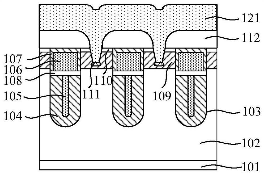
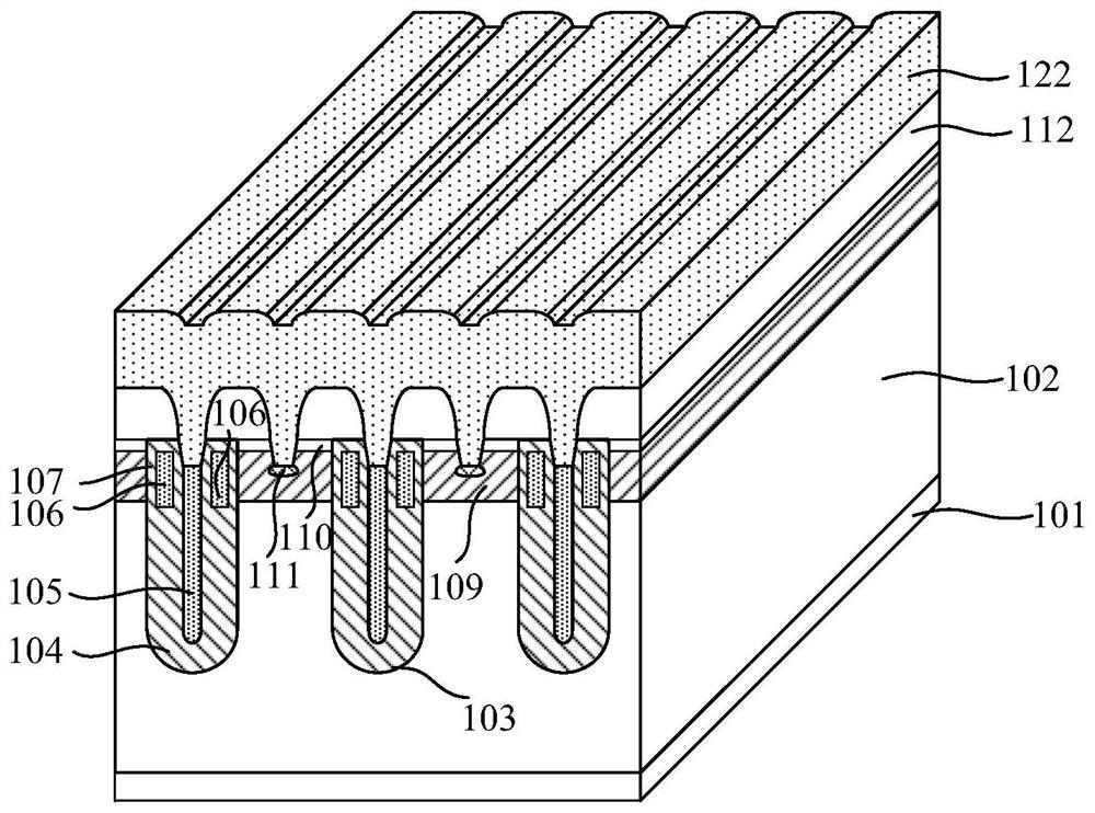
[0091] The power semiconductor device described in the following examples, the shield conductor in one trench has a plurality of leading positions in the longitudinal direction of the groove, solving the two ends of the shield conductor lead in the conventional structure in the longitudinal direction of the groove, two The end distance is too long, resulting in an excessive problem of shield conductor parasitic resistance.

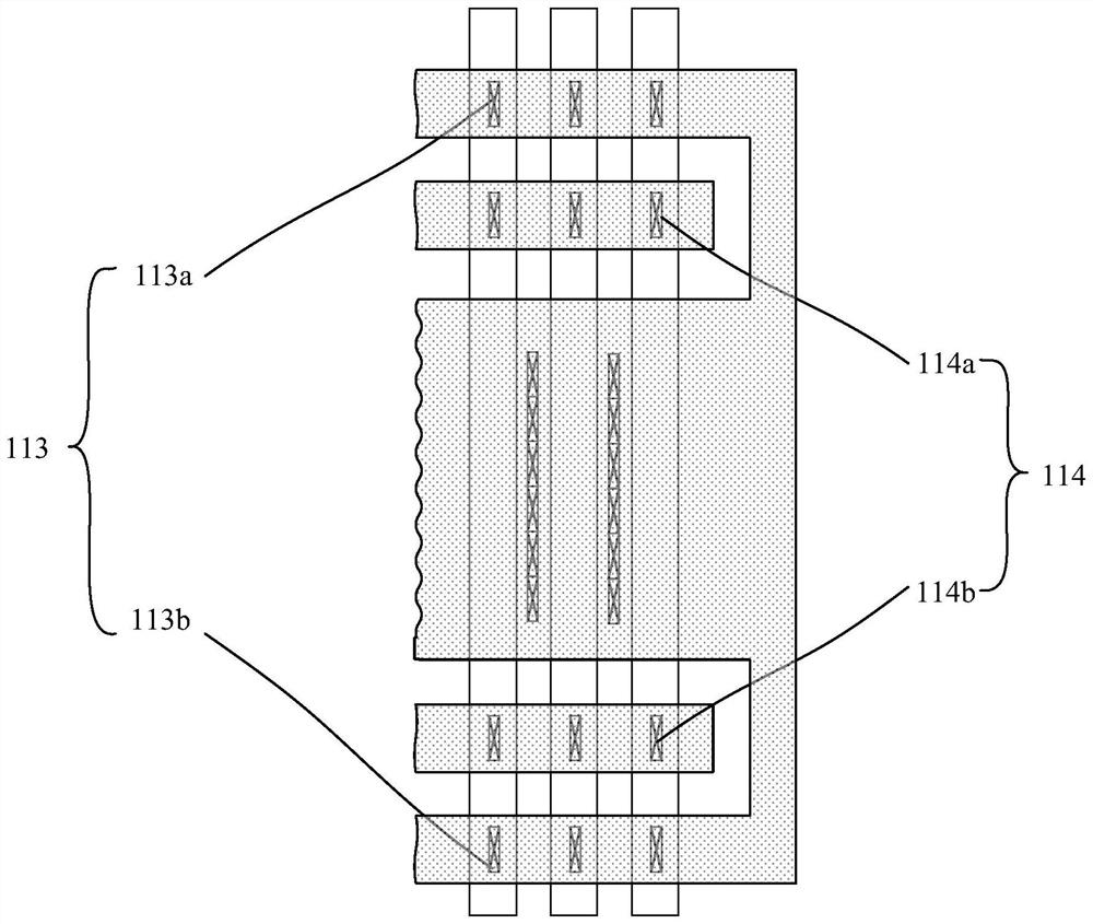
[0092] Figure 4 A layout diagram of a power semiconductor device provided by the first embodiment of the present invention is shown; wherein Figure 5 for Figure 4 The cross-sectional view tak...


PUM

PropertyMeasurementUnit
thicknessaaaaaaaaaa
thicknessaaaaaaaaaa
thicknessaaaaaaaaaa

Abstract

Disclosed are a power semiconductor device and a manufacturing method thereof. Part of a shield conductor of the power semiconductor device is connected to a source electrode, the shield conductor extends from a trench bottom to a position between gate conductors on both sides in a trench at a position electrically connected to the source electrode, the grid conductor and the shielding conductor are separated by an isolation layer, and the shielding conductor is connected with the source electrode; part of the shielding conductor is not connected with the source electrode, and the shielding conductor extends from the bottom of the trench to the area below the gate conductors on the two sides of the upper portion of the trench at the position where the shielding conductor is not electrically connected with the source electrode, so that parasitic resistance of the shielding conductor is reduced, and parasitic resistance is reduced by dozens of times.

Description

[0001] Priority statement [0002] The present application claims 2020104890309, named "Power Semiconductor Device and Its Method", the application date is China Application No. 2020209779322, 2020209779322, is "Power Semiconductor Device", and the application date is 2020 The priority of June 2 (now known as first application). Technical field [0003] The present invention relates to the field of semiconductor manufacturing techniques, and more particularly to a power semiconductor device and a manufacturing method thereof. Background technique [0004] Power semiconductor device is also known as power electronics, including power diode, thyristor, VDMOS (VerticDouble-Diffused Metal Oxide Semiconductor, vertical dual diffusion metal oxide semiconductor) field effect transistor, LDMOS (LDMOS (LDMOS (LDMOS (LDMOS (LDMOS (LDMOS (LDMOS (LDMOS (LDMOS (LDMOS (LDMOS (LDMOS (LDMOS (LDMOS (LDMOS (LDMOS (LDMOS (LDMOS (LDMOS (LDMOS (LDMOS (LDMOS (LDMOS (LDMOS) Semiconductor) Field Effect T...

Claims


Application Information

Patent Timeline
Patent Type & Authority Applications(China)
IPC IPC(8): H01L29/06H01L29/423H01L29/78H01L29/739H01L21/336H01L21/331
CPCH01L29/0603H01L29/0684H01L29/78H01L29/7393H01L29/66477H01L29/66325H01L29/42356
Inventor 张邵华郭广兴杨彦涛
Owner HANGZHOU SILAN MICROELECTRONICS
Why Eureka
Try Eureka