Electrode modification layer, memristor, and preparation and control methods of memristor
An electrode modification layer and memristor technology, which is applied to instruments, electrical components, static memories, etc., can solve the problems of poor consistency of memristor parameters, and achieve the effects of improving consistency, low cost, and simple preparation.
- Summary
- Abstract
- Description
- Claims
- Application Information
AI Technical Summary
Problems solved by technology
Method used
Image

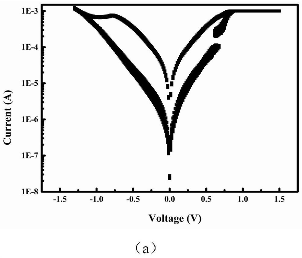
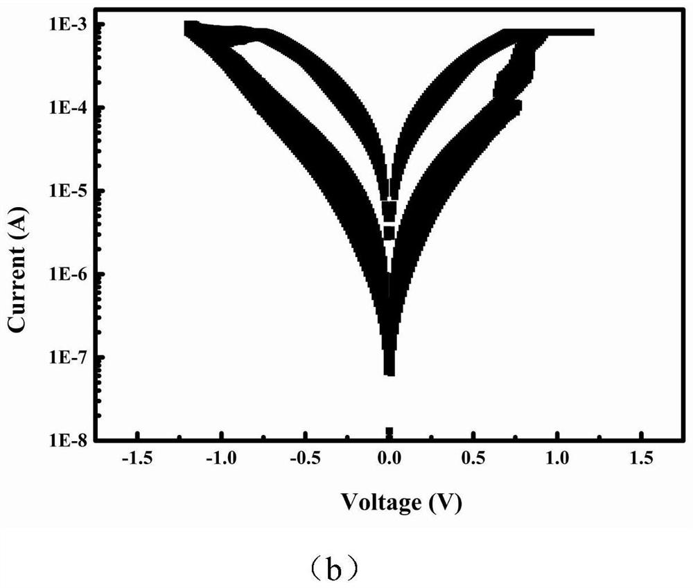
Examples
preparation example Construction
[0051] In the fourth aspect, the present invention also provides the method for preparing the memristor described in the second aspect, comprising the following steps:
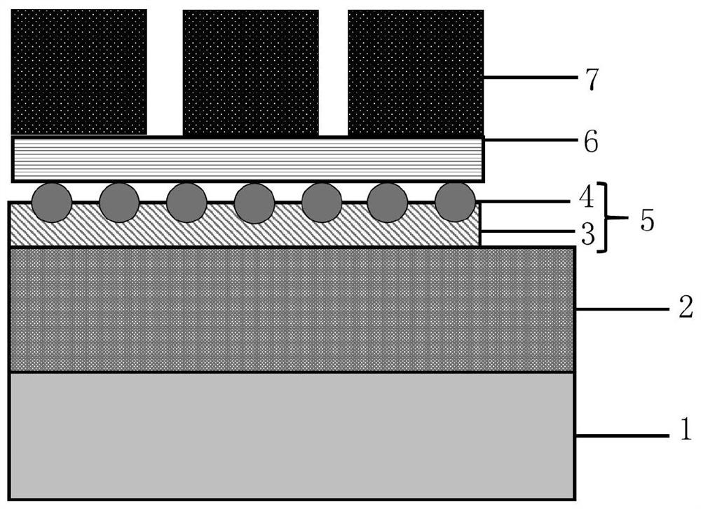
[0052] S1. Provide a substrate, and deposit the first electrode on the surface of the substrate; specifically, the first electrode can be prepared on the substrate by physical vapor deposition; wherein the substrate is preferably SiO 2 single crystal silicon substrate; the physical vapor deposition method is preferably magnetron sputtering; the DC sputtering power is 100-300W, preferably 150W; the sputtering pressure is 0.2-2Pa, preferably 0.5Pa; the inert gas is Ar gas, The sputtering time is 1200s, and the sputtering thickness is preferably controlled to be 100nm.
[0053] S2. An organic electrode layer and a metal nanoparticle layer are sequentially grown on the surface of the first electrode to form a nanocrystalline electrode modification layer; specifically, an organic electrode layer and a metal nanopar...
PUM
| Property | Measurement | Unit |
|---|---|---|
| thickness | aaaaa | aaaaa |
| thickness | aaaaa | aaaaa |
Abstract
Description
Claims
Application Information