Supercharge Your Innovation With Domain-Expert AI Agents!

Ultra-wideband coplanar waveguide transmission line based on silicon-based three-dimensional integration technology

A coplanar waveguide, three-dimensional integration technology, applied in waveguides, waveguide-type devices, circuits, etc., can solve problems such as reduced transmission efficiency, and achieve good grounding effect, low insertion loss, and low return loss.

Inactive Publication Date: 2021-04-06
NO 55 INST CHINA ELECTRONIC SCI & TECHNOLOGYGROUP CO LTD
View PDF5 Cites 2 Cited by
  • Summary
  • Abstract
  • Description
  • Claims
  • Application Information

AI Technical Summary

Problems solved by technology

[0003] In the traditional transmission line design, microstrip line transmission is often used. Its design method and transmission mode are simple. It is equivalent to quasi-TEM wave above 5GHz, which has irreplaceable advantages in the field of low frequency band. However, in the millimeter wave band, microstrip line The line is no longer equivalent to a quasi-TEM wave. During the transmission of radio frequency signals, electromagnetic waves radiate outward, resulting in a decrease in transmission efficiency. Q The value is reduced, so the microstrip line is not suitable for use in the mmWave frequency band

Method used


Image

  • Ultra-wideband coplanar waveguide transmission line based on silicon-based three-dimensional integration technology
  • Ultra-wideband coplanar waveguide transmission line based on silicon-based three-dimensional integration technology
  • Ultra-wideband coplanar waveguide transmission line based on silicon-based three-dimensional integration technology

Examples


Embodiment Construction

[0023] The technical solutions of the present invention will be described in detail below in conjunction with the accompanying drawings.

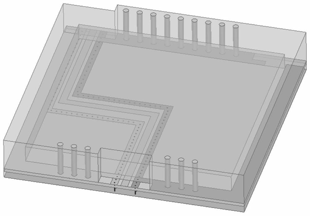
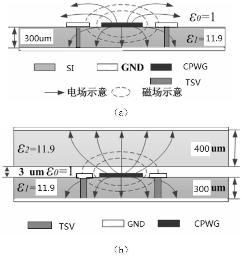
[0024] Such as figure 1 with figure 2 As shown, the present invention designs an ultra-wideband coplanar waveguide transmission line based on silicon-based three-dimensional integration technology, including the relationship between transmission line S parameters and frequency figure 1 , the surface transmission line 5 of the silicon-based adapter board, the TSV through hole 4 arranged inside the first layer of silicon-based adapter board, the second layer of silicon-based substrate 2 located above the first layer of silicon-based adapter board, and the second layer of The third layer of silicon-based substrate 3 above the silicon-based substrate, the TSV light hole 6 inside the second layer of silicon-based substrate and the third layer of silicon-based substrate, the first layer of silicon-based adapter plate 1 and the second layer A f...


PUM

PropertyMeasurementUnit
widthaaaaaaaaaa

Abstract

The invention discloses an ultra-wideband coplanar waveguide transmission line based on a silicon-based three-dimensional integration technology, which comprises a first-layer silicon-based adapter plate, a silicon-based adapter plate surface transmission line, TSV through holes formed in the first-layer silicon-based adapter plate, a second-layer silicon-based substrate located above the first-layer silicon-based adapter plate, a third-layer silicon-based substrate located above the second-layer silicon-based substrate, and TSV light holes formed in the second-layer silicon-based substrate and the third-layer silicon-based substrate. A first bonding layer is arranged between the first silicon-based adapter plate and the second silicon-based substrate, and a second bonding layer is arranged between the second silicon-based substrate and the third silicon-based substrate. The ultra-wideband coplanar waveguide transmission line designed by the invention has the characteristics of low loss, small size, light weight, high power capacity and the like, and can be widely applied to a millimeter wave radio frequency system.

Description

technical field [0001] The invention belongs to the field of microwave silicon-based three-dimensional integrated circuits, and in particular relates to an ultra-wideband coplanar waveguide transmission line. Background technique [0002] The basis for the development of the semiconductor industry was cultivated on technology developed in the 20th century. A relatively new material, a single crystal called silicon, was used in the early 20th century to convert radio communication signals from AC to DC. The semiconductor industry began to grow rapidly in the 1950s to silicon-based production transistor technology, and then the concept of integrated circuits emerged and expanded to how to interconnect different components on a planar silicon material. Circuit integration has continued to increase the number of devices on a chip until today. An important challenge for integrated circuits is the capability of semiconductor manufacturing processes. The rapid technological chang...

Claims


Application Information

Patent Timeline
Patent Type & Authority Applications(China)
IPC IPC(8): H01P3/00H01P3/10
CPCH01P3/00H01P3/10
Inventor 张皓蔡传涛张硕赵磊周潇潇
Owner NO 55 INST CHINA ELECTRONIC SCI & TECHNOLOGYGROUP CO LTD
Features
  • R&D
  • Intellectual Property
  • Life Sciences
  • Materials
  • Tech Scout
  • Unparalleled Data Quality
  • Higher Quality Content
  • 60% Fewer Hallucinations
Learn More