Supercharge Your Innovation With Domain-Expert AI Agents!

Pixel circuit, image sensor, camera module and electronic equipment

A technology for pixel circuits and reading circuits, which is applied in the field of image processing, and can solve problems such as unfavorable pixel miniaturization, reduced pixel performance, and inappropriate

Active Publication Date: 2021-04-06
VIVO MOBILE COMM CO LTD
View PDF5 Cites 6 Cited by
  • Summary
  • Abstract
  • Description
  • Claims
  • Application Information

AI Technical Summary

Problems solved by technology

However, when using Off-Chip (non-chip) technology to practice the pixel-by-pixel HDR modulation method, it is necessary to adopt a complex optical coding exposure control system. This system is not only bulky, but also requires precise calibration between different devices, which consumes high power Suitable for practical use on mobile devices such as mobile phones
When using On-Chip (on-chip) technology to practice the pixel-by-pixel HDR modulation method, the pixel circuit needs to have two or more exposure control signal storage units to control two or more charge storage units, which is not conducive to pixel Miniaturization will reduce the performance of the pixel, such as the fill factor of the pixel (Fill Factor). At the same time, using multiple exposure control signal storage units will have a certain probability that the output exposure control signals are all the same, such as all output high-level signals, Cause the charge generated by the photoelectric conversion device to flow to multiple charge storage regions at the same time and finally make the code exposure fail

Method used


Image

  • Pixel circuit, image sensor, camera module and electronic equipment
  • Pixel circuit, image sensor, camera module and electronic equipment
  • Pixel circuit, image sensor, camera module and electronic equipment

Examples


Embodiment Construction

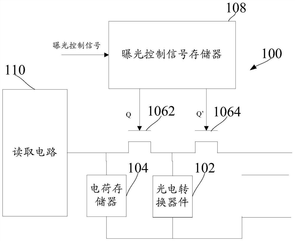
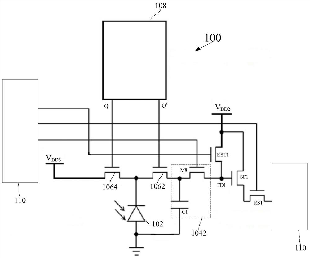
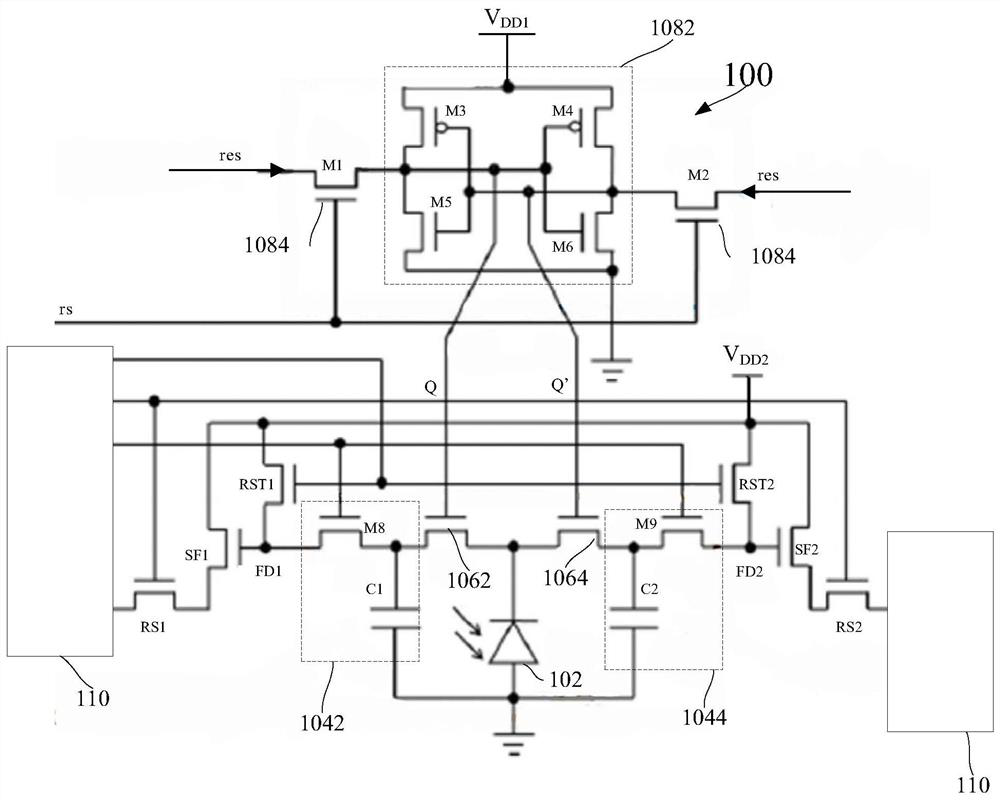
[0027] Embodiments of the present application will be described in detail below, examples of which are shown in the drawings, in which the same or similar reference numerals denote the same or similar elements or elements having the same or similar functions throughout. The embodiments described below by referring to the figures are exemplary, and are only for explaining the present application, and should not be construed as limiting the present application. Based on the embodiments in this application, all other embodiments obtained by persons of ordinary skill in the art without creative efforts fall within the protection scope of this application.

[0028] The features of the terms "first" and "second" in the description and claims of the present application may explicitly or implicitly include one or more of these features. In the description of the present application, unless otherwise specified, "plurality" means two or more. In addition, "and / or" in the specification ...


PUM


Abstract

The embodiment of the invention provides a pixel circuit, an image sensor, a camera module and electronic equipment, and belongs to the technical field of image processing. The pixel circuit comprises a photoelectric conversion device, a charge memory, a first transmission transistor, a second transmission transistor and an exposure control signal memory. Therefore, only one exposure control signal memory is needed, the first transmission transistor and the second transmission transistor are controlled by continuously changing and updating the exposure control signal of each pixel within the exposure time of one frame, the effective exposure time of each pixel can be arranged by the pre-compiled exposure control signal, and a pixel-by-pixel HDR modulation function of the image sensor is realized. On one hand, the problems of size and power consumption in the OffChip technology are avoided; and on the other hand, the size of the pixel can be effectively reduced while the structure of the pixel circuit is simplified, miniaturization of the pixel is facilitated, and the performance of the pixel is improved.

Description

technical field [0001] The present application relates to the technical field of image processing, in particular, to a pixel circuit, an image sensor, a camera module and electronic equipment. Background technique [0002] In a complementary metal-oxide semiconductor image sensor (Complemerntary metal-oxide semiconductor, CMOS), the dynamic range is generally adjusted by changing the exposure time and pixel signal of all pixels for gain adjustment. In high dynamic range (High Dynamic Range, HDR) or wide dynamic range (Wide Dynamic Range, WDR) technology, whether it is multi-frame, line interleaving, or dual gain schemes, all pixels use the same exposure time. The modulation effect of HDR can be changed by the length of exposure time and the adjustment of output signal gain. Since the exposure time of each pixel in the existing HDR technology is the same, the use of HDR results in partial overexposure or underexposure of some pixels in some scenes. [0003] In the related a...

Claims


Application Information

Patent Timeline
IPC IPC(8): H04N5/225H04N5/355H04N5/374
CPCH04N23/57H04N23/55H04N23/54H04N25/59H04N25/76H04N25/771H04N25/53H04N25/779H04N25/585H04N25/78H04N25/57
Inventor 罗轶
Owner VIVO MOBILE COMM CO LTD
Features
  • R&D
  • Intellectual Property
  • Life Sciences
  • Materials
  • Tech Scout
  • Unparalleled Data Quality
  • Higher Quality Content
  • 60% Fewer Hallucinations
Learn More