[0027]The present invention will be described in detail below with reference to the drawings and preferred embodiments, and the objectives and effects of the present invention will become appreciated, and it is understood that the specific embodiments described herein are intended to illustrate only the invention and are not intended to limit the invention.
[0028]Firstly, the technical term explanation is given:
[0029](1) FPGA: Field Programmable Gate Array Scene Programmable Gate Array
[0030](2) RAM: Random Access Memory Random Memory, Here, FPGA internal RAM
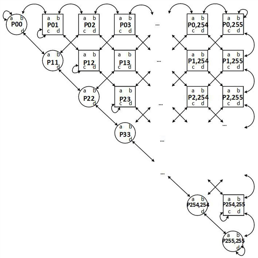
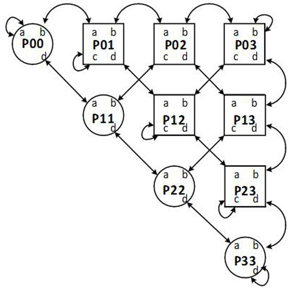
[0031](3) Jacobi: Here specifies the cross-line bilateral Jacqueri rotation, often used by FPGA-based matrix eigenvalue decomposition
[0032](4) BRAM: Block Ram, FPGA internal block RAM
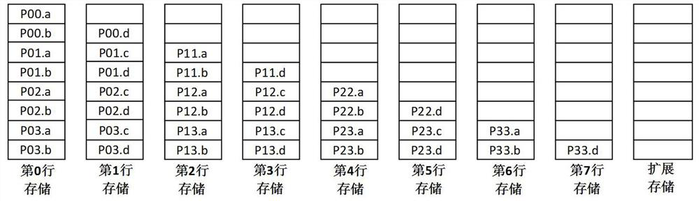
[0033]According to an FPGA-based data storage method, the active symmetrical matrix is 2n row × 2n column, and the number of elements of the upper triangular array structure after the active symmetric matrix is transmitted. Near half of the storage space is free to waste status, and there is a rule that there is a determination of row exchange before and after the Jacobi rotation update. Therefore, the method of the present invention is stored in a failed number matrix, and when the upper triangle array structure is stored after bilateral Jacobi transform, the RAM complementary storage structure is used to replace the common ping-pong structure, and the idle storage is fully utilized, thereby implementing The effect of saving the RAM storage resources close to the original half. In addition, the address address of each row element is sorted from right to left to replace the normal from left to right, retains the ranks exchange law of the original actual active matrix. The specific process is as follows:
[0034]The FPGA is prepared 2n + 1 block, the RAM number I, i∈0 to 2n, the RAM interior site number is j, j∈0 to 2n-1.
[0035]The write storage of the real symmetric matrix includes the steps of:
[0036](1) Convert the real symmetrical matrix into a top triangular array structure, the entire array structure has a total of N (2n + 1) elements, according to the parallel bilateral Jacobi algorithm, each processing unit is a 2 × 2 sub-matrix, the whole The upper triangular array structure contains N (n + 1) / 2 processing units;
[0037](2) Set a RAM storage in each line of the upper triangle array structure in the FPGA, each block RAM starts sequential number from top to 0, that is, the first line data stores in the 0th RAM, the last line of data Stored in the second N-1 RAM, the second N block RAM is additional storage; each RAM internal address is numbered by the right left from 0 and sequentially increments, and sequentially writes each line of the upper triangle array structure to correspond to the corresponding RAM The corresponding address.
[0038]Because the address addressing from each RAM starts from 0, in order to replace the traditional from left to left order, the column rules caused by simply symmetric matrices are simplified by the upper triangle array, and the column rules are disrupted. It can simplify subsequent rancore exchange logic implementation complexity.
[0039]When the upper triangular array structure is bilateral Jacobi transformation, there is a total of N (N + 1) / 2 2 × 2 sub-matrix processing units need to be processed, and the FPGA implementation will be performed in a serial flow water line to save logical resources. The amount of usage. Due to the cross-crosses of the presence rows and columns, the Jacobi calculation update is written back to the same piece RAM overrides the elements that have not yet executed Jacobi rotation calculations, resulting in errors; using a table tennis structure, the RAM storage mode will increase the RAM resource. Therefore, by adding an additional depth and width RAM storage, and numbered 2n, the data exchange with the 0th block RAM is exchanged; other various blocks use structural complementary form, with idle memory cells to store updates The data afterwards, and follow the diagonal exchange rules calculated by Jacobi, so that the data of other addresses will not undermine the data saving the RAM storage resource.
[0040]The data store after the upper triangular array structure is specifically included in the bilateral Jacobi transform includes the steps of:
[0041](1) When i = 0, all data after the I block RAM update is written to the 2N block RAM, and the internal address update law is: the element of the original address J = 2N-1 is written to the new address 0, The element of the original address J = 0 is written to the new address 2n-1, and the remaining original address J is written to the new address 2N-J at the odd element, and the remaining original address J is written to the new address 2N-J for the even number of elements. Place;
[0042](2) When i = 2n-1, the data after the first block RAM update is written in the first block RAM, and the unique element of the original address J = 0 is updated to the new address 2n-1;
[0043](3) When I = 1 to 2n-3 and I are odd, where the original address J = 2n-I-2 element, the updated data is written to the new address i + 1 in the second N-I block RAM; The remaining elements are uniformly written to the 2N- (i + 1) block RAM, and the same RAM internal address update law is performed and the step (1);
[0044](4) When I = 2 ~ 2N-2 and I are even, the updated data is written to the complementary 2N- (I-1) block RAM, and the same RAM internal address update law is performed and step (1) .
[0045]The data storage method of the present invention will be further explained and explained below with a specific embodiment.
[0046]Such asfigure 1 As shown, the upper triangular array structure diagram of the 512 × 512 active symmetric matrix characteristic value decomposition, each element is a real number, the data type is a single precision floating point number, the bit width 32 bits, the FPGA development board selection is Xilinx company The VC707, the FPGA model is XC7VX485T-2FFG1761C, with a total of 2030 blocks containing 18KB of Block RAM. 18kb Bram (2KB for parity) configures the positioning width 32, depth 512, just match the matrix input dimension 512, one 18kb BRAM just stores the corresponding line of the upper triangle array, if the traditional ping Pong RAM storage structure In the actual symmetric matrix feature value decomposition task, only the data exchange is only 1024 blocks of BRAM, and the calculation feature vector also needs to use the equivalent number of RAM storage resources, it has reached 2048 block BRAM, even if there is a small amount of distribution inside the FPGA. The RAM storage is available, and the FPGA layout wiring is also difficult, and the design cannot be passed. Further, only the external DDR3SDRAM storage on the board is stored, and the integral calculation task is implemented through the constant return transfer data between the DDR3 external storage. However, fragmentated data to move back and plus addressed discontinuities, which will result in a reduction in overall calculation, and also put forward demanding requirements for the bandwidth of external storage interfaces.
[0047]Therefore, by using the RAM storage complementary structure of this method, the idle storage is fully utilized, thereby achieving the result of saving the RAM storage resources close to the original half. In addition, the address address of each row of elements from the right to left, retains the ranks exchange law of the original believing matrix, which is the circuit implementation of the row data exchange law before and after the Jacobi rotation of the upper triangle array.
[0048]For the upper triangular array structure of 512 × 512, there is a total of (256 + 1) * 256/2 = 32896 2 × 2 sub-matrix processing units, a total of 512 blocks store for storing elements for storage from top to bottom, Increase the extended storage, RAM bit width 32 bits, depth 512, number 0, 1, 2, ..., 512. The 0th line RAM is full of 512 elements, and 511 elements in the first line RAM, ..., the 511 line RAM has only one element, and the expansion store is automatically all empty.
[0049]To describe and understand, the specific value of the 512 × 512 active symmetrical matrix is decomposed in the specific implementation of the 512 × 512, which will be described in the upper triangular array structure diagram of the 8 × 8 actual symmetric matrix eigenvalue.figure 2 As shown, the principles and processes are exactly the same, except that the size is different.
[0050]When writing storage:
[0051](1) According to the upper triangle array structure, each line is set to each line in each line to each line, each RAM storage is the same, and the elements of each row are used to store the elements of each row. The entire array structure is 8 lines, and 8 blocks need to use RAM storage; additionally adding 1 RAM storage for data exchange stored in line 0, therefore a total of 9 RAM storage;
[0052](2) Each block RAM storage is numbered from top to bottom, and the store number starts from 0, the first first line data stores in the 0th row storage RAM, the last line of data is stored in the 7th line storage The entire upper triangular array structure is stored at the address of the 0th block stored at 0, and the upper left corner of the element is stored at the address 7 stored in the 0th, and the bottom element is stored in the 7th block. 0 At 0; stored from the 0th block RAM to the 7th RAM storage, the number of elements stored from 8 to 1 linearly, the column number corresponds to the address address in the RAM storage; 8 × 8 active symmetric matrix eigenvalue decomposition The upper triangular array structure in the RAM storage in the FPGA storage, such asimage 3 Indicated.
[0053]The upper triangular array structure is specifically: the data storage after bilateral Jacobi transform is:
[0054]According to the data exchange rules and RAM storage formats before and after Jacobi, the row number of the RAM row of RAM on behalf of the RAM is kept unchanged, and the address 0 and addresses 7 two element addresses remain unchanged, the rest of the elements The address address is completed near the parity, that is, the element of the original address 2i-1 is stored in the address 2i after the Jacobi rotation, and the element of the original address 2i is stored in the address 2i-1, i = {1, 2, 3}; When the actual operation, since the Jacobi rotation calculation is performed on the 2 × 2 processing unit pipeline, the 0th line RAM cannot be written back to the 0th row of RAM itself, otherwise the rest has not calculated the updated element is covered, This is to increase the reason for the 8th RAM as a complementary storage. The original address 0 element P03.B obtained after the Jacobi rotation calculation value P03.b 'writes to complementary storage, the 7th address of the 8th RAM Elements of the 0th row storage address is 7, which is written to the address of the 8th RAM after the Jacobi rotation, and the remaining intermediate elements perform the RAM internal address parity cross, such asFigure 4 As shown; the next round iterates, stores the 8th block when making the 0th row, and the content of the original line 0 is invalid, as an extended storage, such cycle processing;
[0055]According to the data exchange rules and the RAM storage format before and after the Jacobi rotation, the last line, the 7th block storage, the storage exchange rules after Jacobi rotation: Seventh block storage only one element, line number, and address address number Keep the constant; the 7th block is stored only one element, while the first block stores only one free element, the two form a complementary structure, such asFigure 5 Indicated.
[0056]According to the data exchange rules before and after Jacobi, the middle line stores, the third line storage, the 5th row of stores, and there is a special element holding line, that is, p01.c, p12.c, p23.c The rows of the remaining elements becomes second, fourth, sixth, each row, except that the address address is unchanged, and the remaining elements perform the crossover of "complementary" in the RAM internal address update law; in the first line storage as an example , The storage name of the first line is written to the second line storage, requiring 6 elements storage locations, but the second line storage itself needs to occupy the storage of 6 elements, resulting in data coverage, and stores with the second line The sixth row of the complementary structure is just six elements of idle position. The two form a complementary structure, so the real first row is written to the sixth line storage after Jacobi rotation, wherein special P01.c Remain unchanged;Figure 6 As shown, special element P01.C keeps the row line unchanged with light gray identity, the first row storage and the second row of storage names, but in fact, it is actually written to the sixth line of the RAM complement structure, where to find The address address executed "complementary" operation.
[0057]According to the data exchange rules and the RAM storage format before and after the Jacobi rotation, the memory exchange laws after the second, fourth, sixth lines are stored in the Jacobi rotation, which becomes first, third, and 5th rows, respectively. For addressing addresses, in addition to address 0 does not change, the remaining addressing addresses actually executes crossover operations of "complementary" in the RAM internal address update law; in the second line storage as an example, such asFigure 7As shown, after the Jacobi rotation calculation is updated, you need to write to the first row storage, requiring 6 elements, and the special element P01.c in the first line S7 requires 7 new elements, which will cause data to be covered, and 7 rows of storage just have seven element storage locations, just in forming complementaries with the first row, the second row is stored in the Jacobi rotation calculation, and the updated value is ultimately written to the 7th row storage location.
[0058]Since a total of 5x4 / 2 = 10 2 × 2 sub-matrix processing units need to be processed, the FPGA implementation is performed in a serial flow line to save logical resources, and then written back to the same block after Jacobi calculation update. Elements that have not yet implemented Jacobi rotation will result in errors; RAM storage uses traditional ping-pong structures, increases double storage resources; use the RAM complementary access structure of the present invention to make the original close half of idle RAM resources Get it, saves nearly half of the FPGA internal RAM storage resources.
[0059]After completing the data exchange of each line, the second round of bilateral Jacobi rotation calculation is continued to the next round of the 5x4 / 2 = 10 2 × 2 sub-matrix, and the above-described data exchange operation is repeated until the convergence condition is satisfied.
[0060]For the upper triangular array structure of 512 × 512, the above method is adopted to increase the 512 block of 18kb of the ping-pong structure by adding 1 18kb BRAM, saving a total of 511 blocks, which requires 1024 blocks of BRAM now only 513 blocks BRAM That is, the BRAM resource uses a decrease in 50%, further can deploy the entire 512 × 512's failed number matrix feature decomposition task to operate at high speeds of the FPGA, and save the constant back-or-transfer intermediate between FPGA and external storage. Calculation results.
[0061]One of ordinary skill in the art will appreciate that only the preferred examples of the invention are not intended to limit the invention, although the foregoing examples have been described in detail, and those skilled in the art will still be The technical solution described in the foregoing examples is modified, or part of the technical features in which part of the technical features are modified. All modifications, equivalents, etc., which are in the spirit and principles of the invention should be included within the scope of the invention.