
Method for processing crimping hole of circuit board

A processing method and circuit board technology, which is applied to printed circuits, printed circuit manufacturing, electrical components, etc., can solve the problems of making crimping holes, increasing the difficulty of making crimping holes, and increasing processing costs, etc.

Pending Publication Date: 2021-04-16
珠海杰赛科技有限公司 +1
View PDF6 Cites 0 Cited by
  • Summary
  • Abstract
  • Description
  • Claims
  • Application Information

AI Technical Summary

Problems solved by technology

[0002] With the continuous expansion of the application of circuit boards, the requirements for all aspects of circuit boards are also increasing. In order to reduce welding and easy replacement of parts, press fit holes are designed. Most of the press fit holes are connected to standard PIN pins. Components, when installing, the PIN foot components are directly inserted without soldering, and the PIN foot components will be squeezed to form a connection with the hole wall. In order to ensure its electrical conductivity and the smooth insertion of the PIN foot components, such holes Position and aperture accuracy requirements are relatively high; at present, the industry generally requires the aperture tolerance of crimping holes to be controlled at ±0.05mm or ±0.025mm, and the hole position tolerance is generally required to be controlled at ±0.05mm, while the hole position tolerance requirement < It is difficult to make crimping holes when the diameter is 0.038mm. At the same time, when the base copper is ≥ 70um and the hole diameter is required to be 0.4-0.5mm, the existing direct drilling method needs to be repeated many times to make test boards, which greatly increases the number of crimping holes. Difficulty in production and increase in processing cost

Method used


Image

  • Method for processing crimping hole of circuit board
  • Method for processing crimping hole of circuit board
  • Method for processing crimping hole of circuit board

Examples


Embodiment Construction

[0019] The following will clearly and completely describe the technical solutions in the embodiments of the present invention with reference to the accompanying drawings in the embodiments of the present invention. Obviously, the described embodiments are only part of the embodiments of the present invention, not all of them. Based on the embodiments of the present invention, all other embodiments obtained by persons of ordinary skill in the art without making creative efforts belong to the protection scope of the present invention.

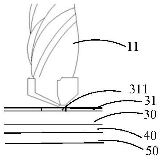
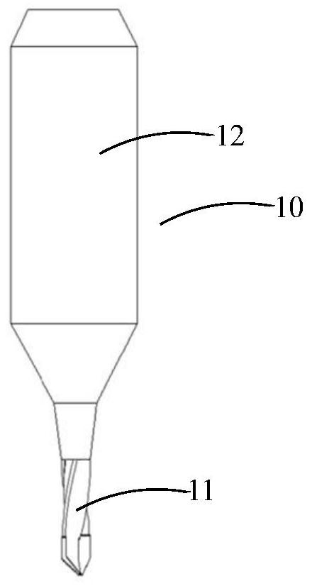
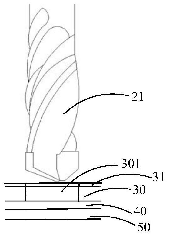
[0020] see Figure 1-Figure 4 , figure 1 It is a schematic diagram of the processing steps of the processing method of the crimping hole of the circuit board in the embodiment of the present invention, figure 2 It is a structural schematic diagram of the first drill in the embodiment of the present invention, image 3 It is a schematic diagram of another processing step of the processing method of the crimping hole of the circuit board in the ...


PUM


Abstract

The invention discloses a method for processing a crimping hole of a circuit board. The method comprises the following steps that a hole position mark of a crimping hole is made on a circuit board; a first drilling tool is adopted to carry out spot drilling at the center of the hole position mark until a copper foil layer of the circuit board is drilled through to form a spot drilling hole, and the thickness of the copper foil layer is larger than or equal to 70 microns; and a second drilling tool is adopted to drill a crimping hole in the center of the spot drilling hole in a heavy hole machining mode. The second drilling tool has the following parameters: the tool diameter is 0.15-6.3 mm, each 0.05 mm is a step, the blade length of the tool bit is 7.3-7.7 mm, and the concentricity of the tool bit and the tool handle is 6-10 micrometers. The first drilling tool has the following parameters: the tool diameter is larger than or equal to 0.4 mm or is a value obtained by subtracting 0.1 mm from the tool diameter of the second drilling tool, the blade length of the tool bit is 1.7-2.1 mm, and the concentricity of the tool bit and the tool handle is 1-4 micrometers. According to the method for processing a crimping hole of a circuit board, the crimping hole is simple to process and high in precision, the processing cost is saved, and the quality of the circuit board is improved.

Description

technical field [0001] The invention relates to the technical field of circuit board processing, in particular to a method for processing a crimping hole of a circuit board. Background technique [0002] With the continuous expansion of the application of circuit boards, the requirements for all aspects of circuit boards are also increasing. In order to reduce welding and easy replacement of parts, press fit holes are designed. Most of the press fit holes are connected to standard PIN pins. Components, when installing, the PIN foot components are directly inserted without soldering, and the PIN foot components will be squeezed to form a connection with the hole wall. In order to ensure its electrical conductivity and the smooth insertion of the PIN foot components, such holes Position and aperture accuracy requirements are relatively high; at present, the industry generally requires the aperture tolerance of crimping holes to be controlled at ±0.05mm or ±0.025mm, and the hol...

Claims


Application Information

Patent Timeline
Patent Type & Authority Applications(China)
IPC IPC(8): H05K3/00
Inventor 何家添唐有军关志锋齐国栋
Owner 珠海杰赛科技有限公司
Learn More