Substrate preparation method, substrate structure, chip packaging method and chip packaging structure

A substrate preparation and substrate technology, which is applied in semiconductor/solid-state device manufacturing, semiconductor/solid-state device components, semiconductor devices, etc., can solve the problem that the depth of opening is not easy to control, affects the yield of chip packaging structure, and easily damages the conductive circuit of the chip To achieve the effect of improving the stability of interface bonding, improving the efficiency of opening holes, and reducing warpage

Active Publication Date: 2021-05-14
广东佛智芯微电子技术研究有限公司
View PDF6 Cites 1 Cited by
  • Summary
  • Abstract
  • Description
  • Claims
  • Application Information

AI Technical Summary

Problems solved by technology

During the opening process, the depth of the opening is not easy to control, and it is easy to damage the chip or break down other conductive lines, which affects the yield of the chip packaging structure

Method used


Image

  • Substrate preparation method, substrate structure, chip packaging method and chip packaging structure
  • Substrate preparation method, substrate structure, chip packaging method and chip packaging structure
  • Substrate preparation method, substrate structure, chip packaging method and chip packaging structure

Examples


Embodiment 1

[0104] The chip packaging method of this embodiment includes the following steps:

[0105] S10. Prepare the first sub-substrate:

[0106] S10a, providing a first glass substrate 11, pasting a first photosensitive dry film on one side of the first glass substrate 11, forming several windows after exposure and development;

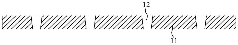
[0107] S10b. Perform laser focus modification on the first glass substrate 11 exposed to the window, and then use a hydrofluoric acid solution to etch the laser focus modification area to obtain a TGV through hole 12 penetrating through the first glass substrate 11, refer to figure 1 ;

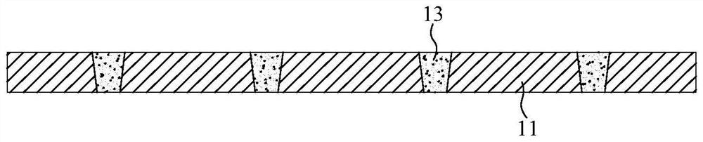
[0108] S10c, making the first conductive post 13 in the TGV through hole 12 by electroplating, and making the two ends of the first conductive post 13 respectively flush with both sides of the first glass substrate 11, and then removing the remaining first photosensitive dry film ,refer to figure 2 ;

[0109] S20. Prepare the second sub-substrate:

[0110] S20a, provide...

Embodiment 2

[0139] The chip packaging method of this embodiment is basically the same as the first embodiment above, the difference lies in the substrate preparation method, and the substrate preparation method specifically includes the following steps:

[0140] S10. Prepare the first sub-substrate:

[0141] S10a, providing a first glass substrate 11, pasting a first photosensitive dry film on one side of the first glass substrate 11, forming several windows after exposure and development;

[0142] S10b. Perform laser focus modification on the first glass substrate 11 exposed to the window, and then use ammonium bifluoride solution to etch the laser focus modification area to obtain a TGV through hole 12 that runs through the first glass substrate 11. Refer to figure 1 ;

[0143] S10c, making the first conductive column 13 in the TGV through hole 12 by electroplating, and making one end surface of the first conductive column 13 flush with one side of the first glass substrate 11, and the...


PUM


Abstract

The invention discloses a substrate preparation method, a substrate structure, a chip packaging method and a chip packaging structure. The substrate preparation method comprises the steps that a first glass substrate is provided, a plurality of first conductive columns are embedded into the first glass substrate, and the two end faces of each first conductive column are exposed out of the two sides of the first glass substrate in the thickness direction of the first glass substrate respectively to prepare a first sub-substrate; a second glass substrate is provided, a line groove is formed in one side of the second glass substrate, a plurality of via holes penetrating through the second glass substrate are formed in the line groove, second conductive columns are manufactured in the via holes, first rewiring layers connected with the second conductive columns are manufactured in the line groove, and a second sub-substrate is manufactured; the first sub-substrate and the second sub-substrate are attached together, the first conductive columns are electrically connected with the first rewiring layer, and the substrate structure is manufactured. The conductive circuit of the substrate structure prepared by the method is good in connection stability, the preparation method is simple, subsequent chip mounting is facilitated, and the product yield is improved.

Description

technical field [0001] The invention relates to the technical field of integrated circuits, in particular to a substrate preparation method and a substrate structure, a chip packaging method and a chip packaging structure. Background technique [0002] With the trend of miniaturization and integration of electronic products, the high density of microelectronic packaging technology has gradually become the mainstream in the new generation of electronic products. In order to comply with the development of the new generation of electronic products, especially the development of mobile phones, notebooks, smart wearable devices and other products, chips are developing in the direction of higher density, faster speed, smaller size and lower cost. [0003] During the packaging process, due to the difference in thermal expansion coefficients of materials such as plastic, silicon, and metal, the volume changes of these materials are not synchronized, resulting in stress and warping. ...

Claims


Application Information

Patent Timeline
Patent Type & Authority Applications(China)
IPC IPC(8): H01L21/48H01L23/498
CPCH01L21/486H01L21/4857H01L23/49822H01L23/49833H01L23/49827H01L23/49838H01L2224/02331H01L2224/02381H01L2224/02379H01L2224/02333
Inventor 杨斌崔成强罗绍根
Owner 广东佛智芯微电子技术研究有限公司
Why Eureka
Try Eureka