Mos transistor with gate protection diode
A technology of MOS transistors and protective diodes, which is applied in the field of semiconductor integrated circuits, can solve problems such as leakage performance inconsistencies, and achieve the effect of preventing adverse effects and preventing forward bias
Active Publication Date: 2021-05-28
HUA HONG SEMICON WUXI LTD +1
View PDF2 Cites 2 Cited by
- Summary
- Abstract
- Description
- Claims
- Application Information
AI Technical Summary
Problems solved by technology
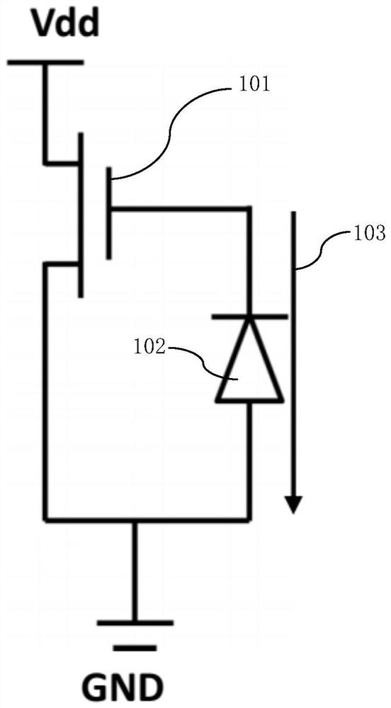
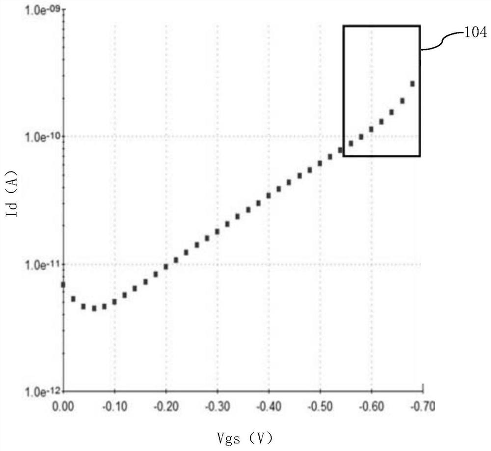
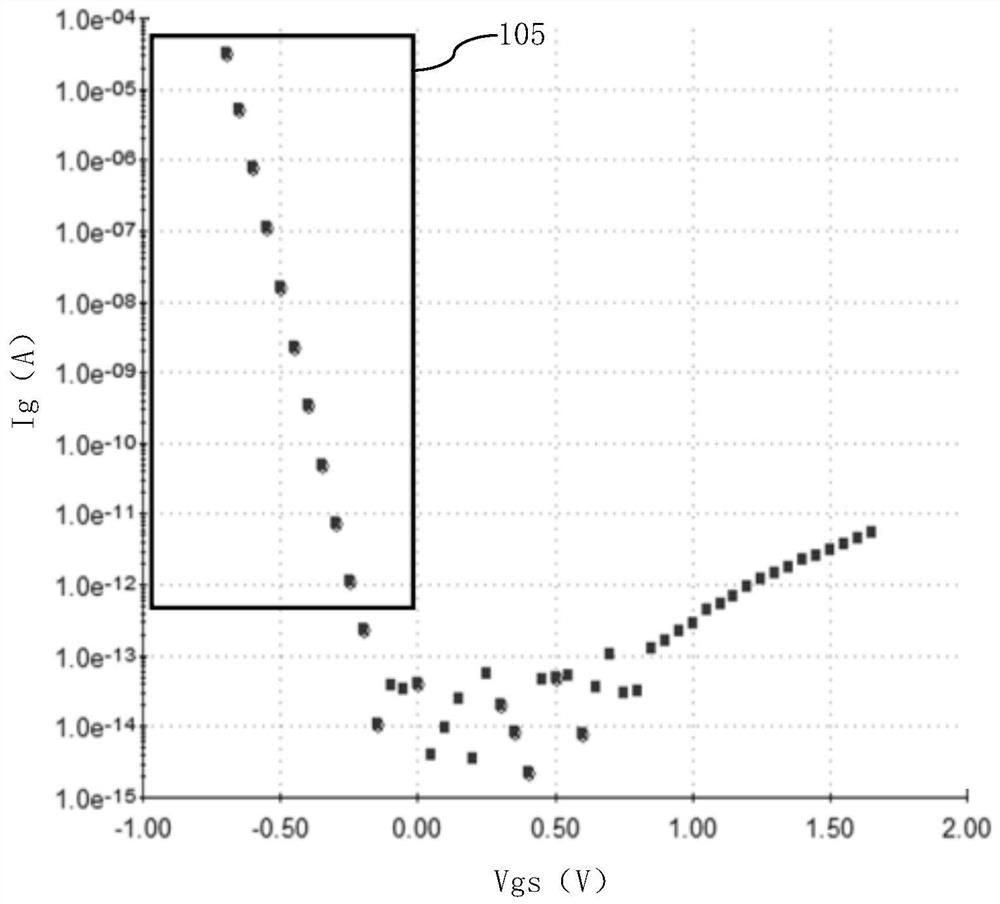
[0008] Figure 2A and Figure 2B The test results obviously do not match the actual leakage performance of NMOS101
Method used
View moreImage
Smart ImageViewing Examples

Examples
no. 1 example 1
[0100] Like the first embodiment of the present invention, the second embodiment of the present invention enables the gate protection diode 202 to not be forward-biased when the gate-source voltage of the first PMOS 201 is any value. This is beneficial for accurate electrical testing, especially leakage testing, of the first PMOS 201 . During the IV test process of the first PMOS201, the gate voltage applied to the gate structure of the first PMOS201 is scanned from greater than the power supply voltage Vdd to less than the power supply voltage Vdd; the GIDL leakage and gate leakage of the first PMOS201 The characteristics are tested when the gate voltage of the first PMOS 201 is greater than the power supply voltage Vdd.
Login to View More PUM
 Abstract
The invention discloses an MOS transistor with a gate protection diode, which is characterized in that the carrier type of a conducting channel of the MOS transistor is a first conducting type, and a second conducting type doped region of the gate protection diode is connected with a source region of the MOS transistor; the first conductive type doped region of the gate protection diode is connected with the gate structure of the MOS transistor through a first switch; when the MOS transistor is conducted by the gate-source voltage of the MOS transistor, the first switch is also conducted, and the gate protection diode provides a discharge path for plasma charges of the gate structure of the MOS transistor; and the first switch prevents the gate protection diode from generating positive bias when the gate-to-source voltage of the MOS transistor turns off the MOS transistor. The grid protection diode can be prevented from generating positive bias, accumulation of plasma charges in a grid structure caused by plasma damage in the CMOS manufacturing process can be eliminated, meanwhile, GIDL and grid leakage current can be accurately measured, and the accuracy of an SPICE model can be improved.
Description
technical field [0001] The invention relates to a semiconductor integrated circuit, in particular to a MOS transistor with gate protection diodes. Background technique [0002] In the CMOS process, the plasma generated in the plasma-enhanced chemical vapor deposition (PECVD), reactive ion etching (RIE) and other processes that require the use of plasma (plasma) will remain in the gate structure such as the gate structure during the manufacture of MOS devices. pole structure on the polysilicon gate. The residual plasma charge on the polysilicon gate will affect the performance of the device. In the prior art, a gate protection diode is often used to eliminate the plasma charge caused by the plasma damage. A path for plasma charge discharge is provided through the gate protection diode. Such as figure 1 Shown is a circuit diagram of an existing MOS transistor with a gate protection diode; taking the MOS transistor as NMOS as an example, it includes: [0003] NMOS101, inclu...
Claims
Login to View More Application Information
Patent Timeline
 Patent Type & Authority Applications(China)
IPC IPC(8): H03K17/687
CPCH03K17/687
Inventor 汤茂亮张昊
Owner HUA HONG SEMICON WUXI LTD