


Quick Research
Generate reliable direction feasibility study reports for your R&D in just a few steps.

Technical Q&A
Discover and master advanced knowledge NOW. Basics, ideas, possibilities, all at once.

Find Solutions
As an expert in R&D theories, this can generate solutions to your technical problems instantly.

Evaluate Feasibility
Analyze your overall solution with one click, know your potential R&D risks in advance.

Monitor Landscape
Get weekly tech updates, stay abreast of the latest tech innovations and key insights.
Integrated system for monocrystalline silicon epitaxial wafer detection
An integrated system and epitaxial wafer technology, applied in the direction of measuring devices, instruments, etc., can solve the problems of low detection efficiency and cumbersome detection process of epitaxial wafers, and achieve the effect of easy detection, improved detection efficiency and convenient detection
- Summary
- Abstract
- Description
- Claims
- Application Information
AI Technical Summary
Problems solved by technology
Method used
Image

Examples
Embodiment
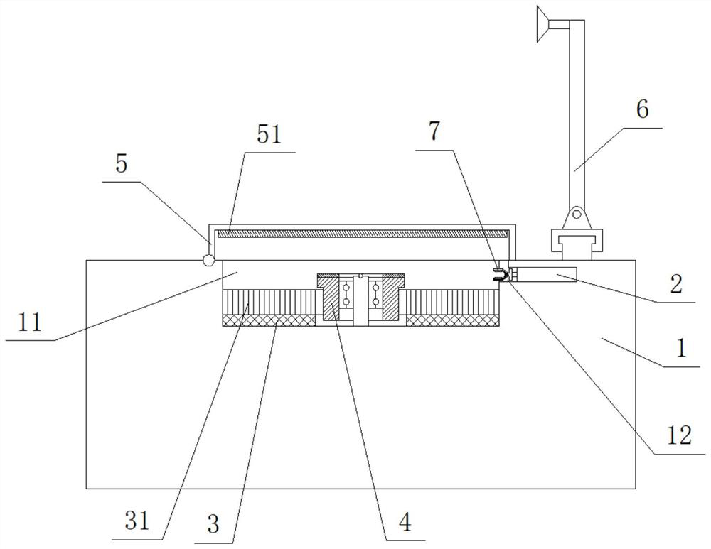
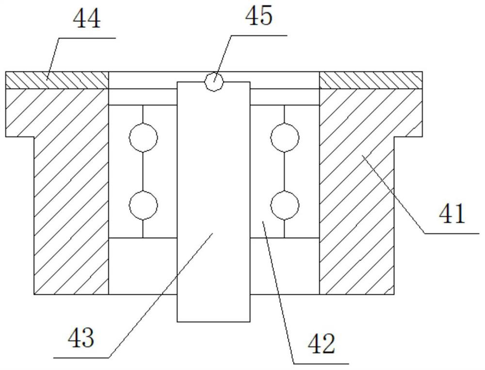
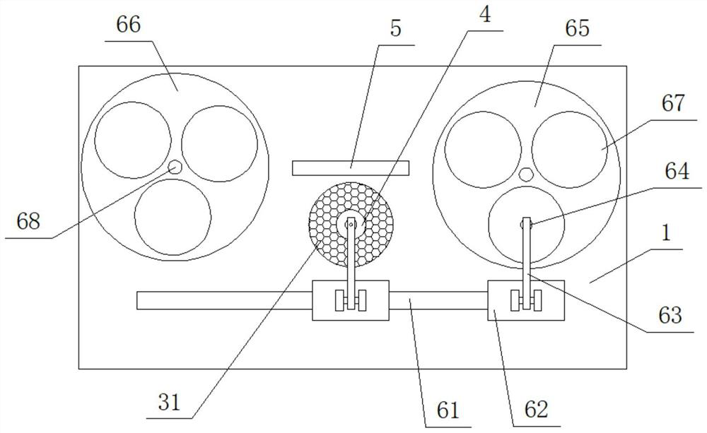
[0029] Such as Figure 1 to Figure 6 As shown, the integrated system for detection of single crystal silicon epitaxial wafers provided by this embodiment includes a workbench 1, a protective cover 5, a feeding device 6 and a detection mechanism 7, and the workbench 1 is processed with a placement cavity 11 for placing epitaxial wafers. A lamp panel 3 is placed on the surface of the placement cavity 11. The lamp panel 3 is composed of a plurality of LED lamp discharge materials. A honeycomb cover 31 is installed on the lamp panel 3. The honeycomb cover 31 is ring-shaped, and the honeycomb cover 31 is made of black material. Its purpose is to make the light emitted by the lamp panel 3 irradiate vertically upwards, so as to quickly read the orthographic area of the single crystal silicon epitaxial wafer, thereby improving the speed of measuring the area of the single crystal silicon epitaxial wafer, and place it in the middle of the cavity 11. A rotary table 4 is installed, a...
PUM
 Abstract
Description
Claims
Application Information
 - R&D Engineer
- R&D Manager
- IP Professional
- Industry Leading Data Capabilities
- Powerful AI technology
- Patent DNA Extraction
Browse by: Latest US Patents, China's latest patents, Technical Efficacy Thesaurus, Application Domain, Technology Topic, Popular Technical Reports.
© 2024 PatSnap. All rights reserved.Legal|Privacy policy|Modern Slavery Act Transparency Statement|Sitemap|About US| Contact US: help@patsnap.com