A deep silicon detector module with integrated preamplifier circuit

A pre-amplification circuit and detector technology, applied in the field of detectors, can solve the problems of low detector definition, affecting the definition, occupying a large space, etc., and achieve the effect of reduced volume and weight, reliable design principle, and tight arrangement

Active Publication Date: 2022-05-17
核芯光电科技(山东)有限公司
View PDF6 Cites 0 Cited by
  • Summary
  • Abstract
  • Description
  • Claims
  • Application Information

AI Technical Summary

Problems solved by technology

[0005] For the above-mentioned traditional CT detectors in the prior art, the resolution is low, the volume is large, and the resolution is limited, while the new generation of semiconductor CT is arranged in two layers and read on both sides, which takes up a lot of space, is large in size, affects the definition, and is complicated to install. Defect, the present invention provides a deep silicon detector module with integrated preamplifier circuit to solve the above technical problems

Method used


Image

  • A deep silicon detector module with integrated preamplifier circuit
  • A deep silicon detector module with integrated preamplifier circuit
  • A deep silicon detector module with integrated preamplifier circuit

Examples


Embodiment 1

[0051] The invention provides a deep silicon detector module integrating a preamplifier circuit, including at least two detector chips;

[0052] The detector chips are stacked, and the adjacent detector chips are insulated;

[0053] The detector chip is provided with a light-receiving side, the light-receiving side of each detector chip is arranged on the same arc surface, the adjacent detector chips are arranged at an angle, and the angle between the adjacent detector chips is smaller than the set threshold;

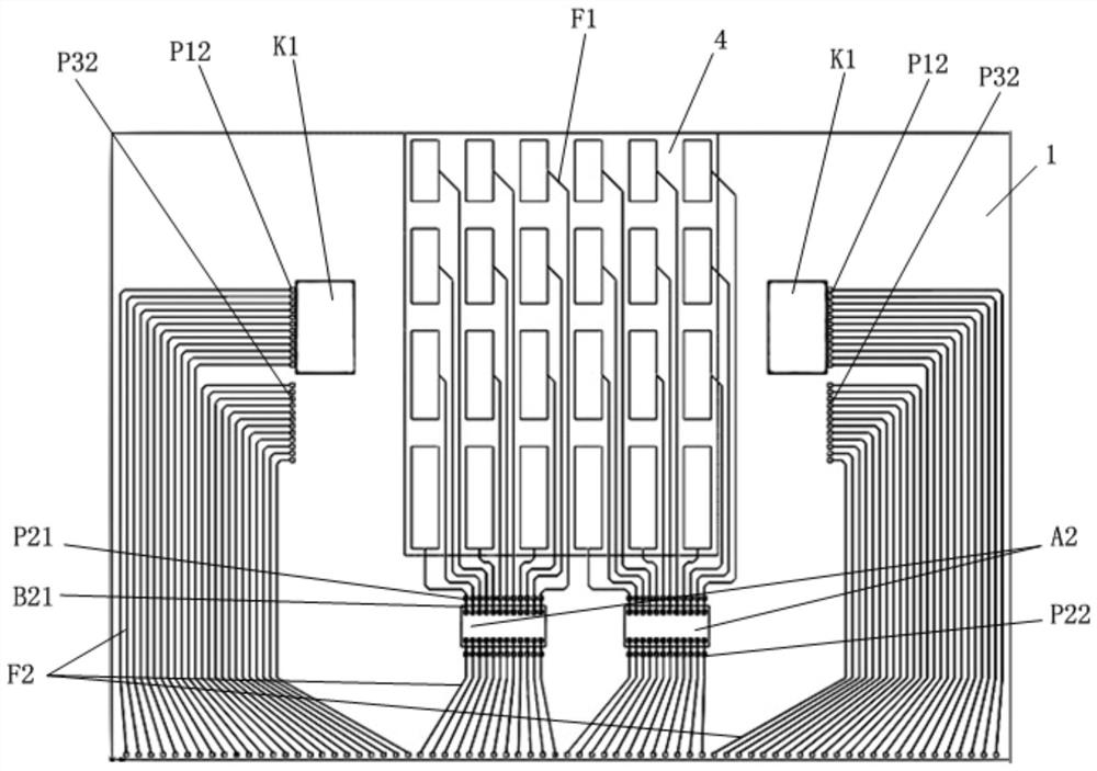
[0054] The detector chip includes a sensitive area unit, a preamplification processing chip integrated area unit, a bonding area unit and an opening area unit;

[0055] The sensitive area unit is arranged on the light-receiving side of the detector chip; the sensitive area unit includes a number of silicon microstrips, each silicon microstrip is parallel, and is distributed along the edge of the light-receiving side of the detector chip to the inside of the detector chi...

Embodiment 2

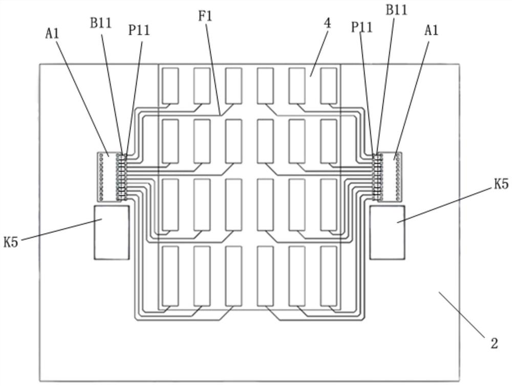
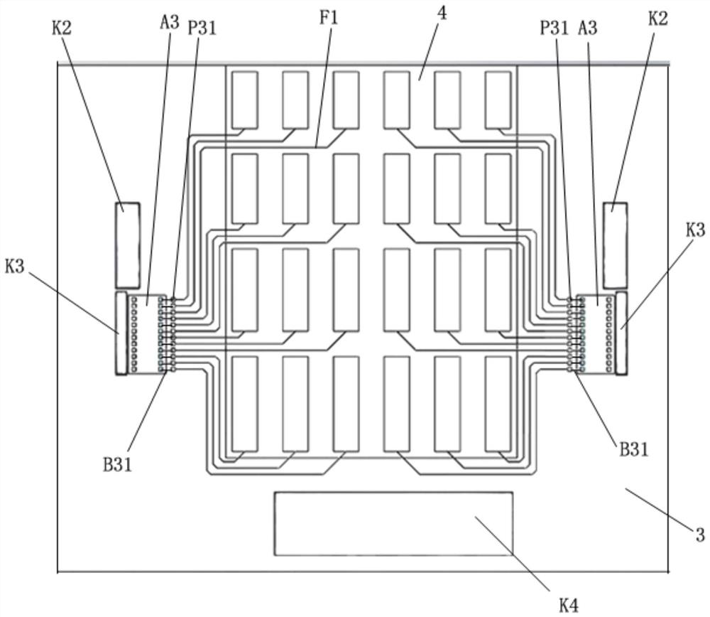
[0088] Such as figure 1 , figure 2 and image 3 As shown, the present invention provides a deep silicon detector module integrating a preamplifier circuit, including three detector chips; the detector chip is divided into a main detector chip and a slave detector chip; wherein, the three detector chips are Master detector chip 1, first slave detector chip 2 and second slave detector chip 3;

[0089] Three detector chips are stacked, wherein the first slave detector chip 2 is located at the bottom layer, the main detector chip 1 is located at the middle layer, and the second slave detector chip 3 is located at the uppermost layer, and the adjacent detector chips are insulated set up;

[0090] The three detector chips are all equipped with a light-receiving side, and the light-receiving sides of the three detector chips are arranged on the same arc surface, and the main detector chip 1 is set at an angle to the first slave detector chip 2 and the second slave detector chip 3...


PUM

PropertyMeasurementUnit
thicknessaaaaaaaaaa

Abstract

The invention provides a deep silicon detector module integrating a preamplifier circuit, which includes at least two detector chips; each detector chip is stacked, and adjacent detector chips are arranged at an angle; the detector chip includes a sensitive area, an integrated area, bonding area and opening area unit; the sensitive area unit includes silicon microstrips composed of several photoelectric units; the integrated area unit includes an ASIC chip, and the ASIC chip includes input and output pins; the bonding area includes input and output lead pads and Bonding aluminum wire; connecting the input lead pad to the photoelectric unit and the input pin; connecting the output lead pad to the output pin of the ASIC chip on the same layer, or connecting the output lead pin of the ASIC chip on the adjacent layer; opening area , used to avoid the interlayer wiring between the output pins of the ASIC chip and the output lead pads of the adjacent layer, and at the same time avoid the bonding aluminum wire between the ASIC chip of the adjacent layer and the pads and the pins of the ASIC chip.

Description

technical field [0001] The invention belongs to the technical field of detectors, and in particular relates to a deep silicon detector module integrating a preamplifier circuit. Background technique [0002] At present, the detector used in traditional CT is a scintillator detector, and a photodiode array is integrated below it. This kind of scintillator detector has low imaging resolution and cannot provide color images. The equipment is bulky and heavy; and it is limited by the size of the detector pixel. , with limited spatial resolution. [0003] The new generation of semiconductor detectors for CT uses a single chip as the smallest unit. When arranged, it adopts a two-layer layout. The space is large, and the readout circuits are distributed on both sides, resulting in a large detector; the second is that there is an optical path difference between the X-rays received by the front and rear layers of the semiconductor detector, and the received X-rays are inconsistent, ...

Claims


Application Information

Patent Timeline
Patent Type & Authority Patents(China)
IPC IPC(8): H01L27/146H01L25/16
CPCH01L27/14634H01L27/14636H01L27/14658H01L25/167Y02P70/50
Inventor 刘鹏
Owner 核芯光电科技(山东)有限公司
Why Eureka
Try Eureka