High temperature resistant type Ⅱ optical waveguide processing method, system and high temperature resistant type Ⅱ double wire waveguide

A processing method and high temperature resistant technology, applied in metal processing equipment, optics, manufacturing tools, etc., to achieve the effect of low transmission loss and fast processing method

Active Publication Date: 2022-06-17
PEKING UNIV
View PDF0 Cites 0 Cited by
  • Summary
  • Abstract
  • Description
  • Claims
  • Application Information

AI Technical Summary

Problems solved by technology

[0005] The embodiment of the present application provides a high temperature resistant type II optical waveguide processing method, system and high temperature resistant type II double-wire waveguide, which can solve the problem of how to quickly prepare a high temperature resistant and low loss type II double wire waveguide

Method used


Image

  • High temperature resistant type Ⅱ optical waveguide processing method, system and high temperature resistant type Ⅱ double wire waveguide
  • High temperature resistant type Ⅱ optical waveguide processing method, system and high temperature resistant type Ⅱ double wire waveguide
  • High temperature resistant type Ⅱ optical waveguide processing method, system and high temperature resistant type Ⅱ double wire waveguide

Examples


Embodiment Construction

[0046] The technical solutions in the embodiments of the present application will be clearly and completely described below with reference to the accompanying drawings in the embodiments of the present application. Obviously, the described embodiments are part of the embodiments of the present application, not all of the embodiments. Based on the embodiments in the present application, all other embodiments obtained by those of ordinary skill in the art without creative work fall within the protection scope of the present application.

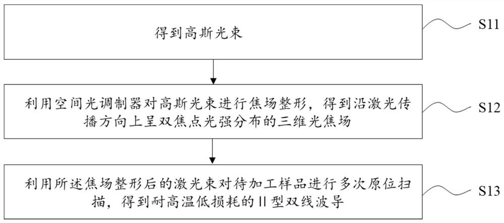
[0047] figure 1 It is a flow chart of the steps of the high temperature resistant type II optical waveguide processing method in the embodiment of the present application, such as figure 1 As shown, the steps of preparing the high temperature resistant type II optical waveguide in the embodiment of the present application are as follows:

[0048] The high temperature resistant type II optical waveguide prepared in the present application has t...


PUM

PropertyMeasurementUnit
refractive indexaaaaaaaaaa

Abstract

The application provides a high temperature resistant type II optical waveguide processing method and system and a high temperature resistant type II double-wire waveguide, which relate to the technical field of waveguide preparation. The invention can solve the problem of how to quickly obtain the high temperature-resistant type II double-wire waveguide. The method includes: obtaining a Gaussian beam; using a spatial light modulator to perform focal field shaping on the Gaussian beam to obtain a three-dimensional optical focal field with bifocal light intensity distribution along the laser propagation direction; using the laser beam after focal field shaping to treat The processed samples were scanned multiple times in situ to obtain a type II double-wire waveguide with high temperature resistance and low loss.

Description

technical field [0001] The present application relates to the technical field of optical waveguide preparation, in particular to a high temperature resistant type II optical waveguide processing method, system and high temperature resistant type II bifilar waveguide. Background technique [0002] The waveguide is the basic unit of the integrated chip. For extreme fields such as aerospace, the device is often required to withstand high temperatures. However, the optical waveguides often used by researchers for direct writing of glass and polymer materials have a limited operating temperature. High-performance optical waveguides and integrated photonic devices are very necessary in extreme fields such as aerospace. Type I waveguide is easy to be erased at high temperature and difficult to retain, so the related field adopts type II bifilar waveguide induced by stress. [0003] The waveguide prepared by femtosecond laser direct writing has the advantages of high flexibility an...

Claims


Application Information

Patent Timeline
Patent Type & Authority Patents(China)
IPC IPC(8): G02B27/09B23K26/06B23K26/082B23K26/50B23K26/70
CPCB23K26/082B23K26/0665B23K26/50B23K26/702G02B27/09
Inventor 闫霖玉龚旗煌李焱李萌
Owner PEKING UNIV
Why Eureka
Try Eureka