Preparation method of one-dimensional cadmium sulfoselenide semiconductor nanowire, nanowire and device

A cadmium sulfide selenide and nanowire technology, which is applied in semiconductor devices, chemical instruments and methods, nanotechnology, etc., can solve problems such as lack of good controllability

Pending Publication Date: 2021-06-04
SUZHOU R&D CENT OF NO 214 RES INST OF CHINA NORTH IND GRP
View PDF4 Cites 0 Cited by
  • Summary
  • Abstract
  • Description
  • Claims
  • Application Information

AI Technical Summary

Problems solved by technology

In the gas-liquid-solid growth mode, the melting point of the catalyst for growing nanowires is lower than the temperature at which nanowires grow, and th

Method used


Image

  • Preparation method of one-dimensional cadmium sulfoselenide semiconductor nanowire, nanowire and device
  • Preparation method of one-dimensional cadmium sulfoselenide semiconductor nanowire, nanowire and device
  • Preparation method of one-dimensional cadmium sulfoselenide semiconductor nanowire, nanowire and device

Examples


Embodiment Construction

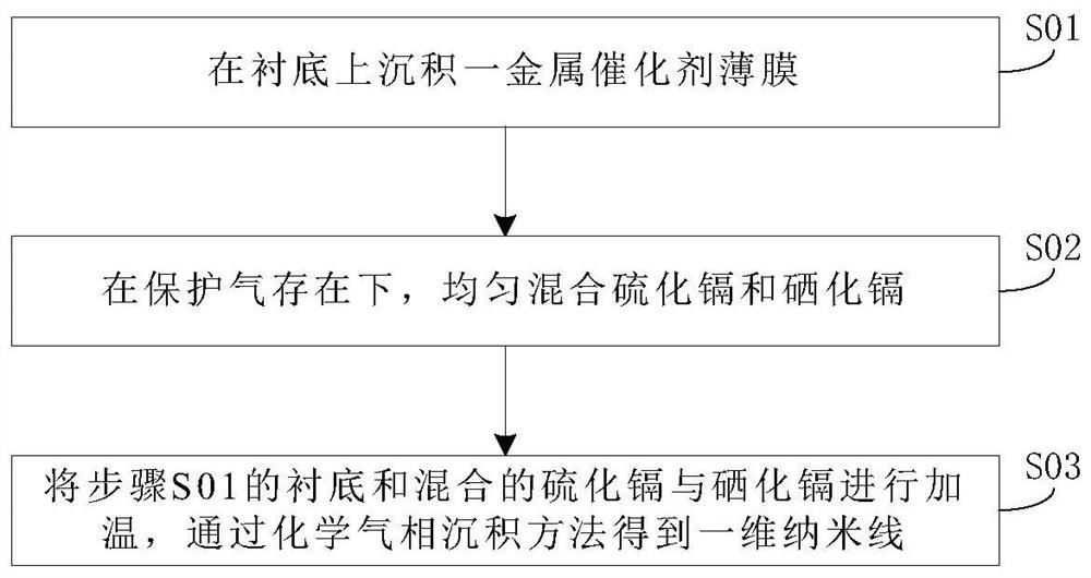
[0031] In order to make the object, technical solution and advantages of the present invention clearer, the present invention will be further described in detail below in combination with specific embodiments and with reference to the accompanying drawings. It should be understood that these descriptions are exemplary only, and are not intended to limit the scope of the present invention. Also, in the following description, descriptions of well-known structures and techniques are omitted to avoid unnecessarily obscuring the concept of the present invention.

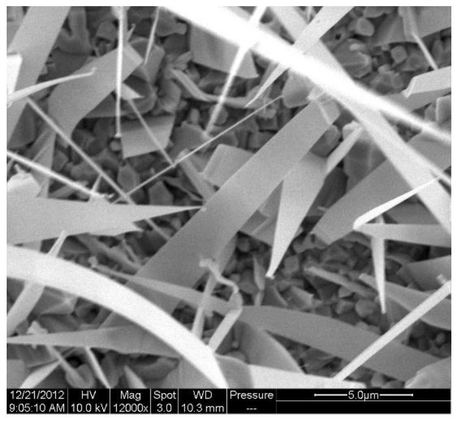
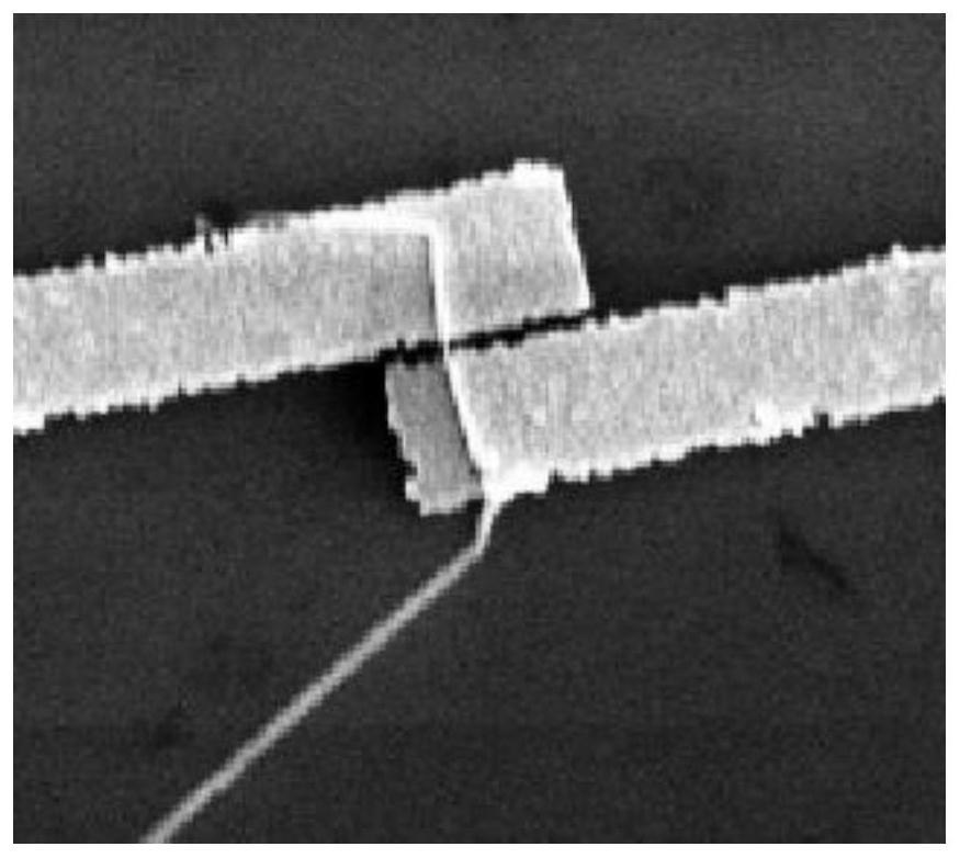
[0032] Such as figure 1 Shown, a kind of preparation method of one-dimensional cadmium sulfur selenide semiconductor nanowire of the present invention, the nanowire growth mechanism is gas-solid growth mechanism, comprises the following steps:

[0033] S01: depositing a metal catalyst thin film on the substrate;

[0034] S02: In the presence of protective gas, uniformly mix cadmium sulfide and cadmium selenide;

[0035...


PUM

PropertyMeasurementUnit
Thicknessaaaaaaaaaa
Thicknessaaaaaaaaaa

Abstract

The invention discloses a preparation method of a one-dimensional cadmium selenide semiconductor nanowire. The preparation method comprises the steps that a metal catalyst thin film is deposited on a substrate; in the presence of protective gas, cadmium sulfide and cadmium selenide are uniformly mixed; and the substrate on which the catalyst thin film is deposited and the cadmium sulfide and the cadmium selenide which are mixed are heated, and the nanowire is obtained through a chemical vapor deposition method. By adopting the chemical vapor deposition method, large-area batch growth can be achieved, the growth direction and length of the semiconductor nanowire can be effectively controlled, and the carrier mobility of the semiconductor nanowire can be remarkably improved. A manufactured photoelectric detector is excellent in performance.

Description

technical field [0001] The invention relates to the technical field of nanomaterial synthesis, in particular to a preparation method of a one-dimensional cadmium sulfur selenide semiconductor nanowire, a one-dimensional cadmium sulfur selenide semiconductor nanowire and a device including the one-dimensional cadmium sulfur selenide semiconductor nanowire. Background technique [0002] Semiconductor nanowires / ribbons play an important role in electronic, optoelectronic and nanoelectromechanical devices, as well as additives in other materials, wiring in integrated circuits, field emission devices and nanosensors. II-VI semiconductor nanowires have unique optoelectronic properties and are very promising to become the next generation of high-performance optoelectronic materials. In many optoelectronic device research fields, changing the carrier mobility of semiconductor nanowires by doping can greatly improve their optoelectronic properties. The mobility of semiconductor nano...

Claims


Application Information

Patent Timeline
IPC IPC(8): C23C16/30C30B29/48C30B29/62C30B25/02B82Y40/00H01L31/0296H01L31/0352H01L31/18
CPCC23C16/306C30B29/48C30B29/62C30B25/005C30B25/02B82Y40/00H01L31/02966H01L31/035227H01L31/1832H01L31/1836H01L31/1896Y02P70/50
Inventor 戴放沈吉刘彬常维静徐叔喜王仕鑫
Owner SUZHOU R&D CENT OF NO 214 RES INST OF CHINA NORTH IND GRP
Why Eureka
Try Eureka