
Doping device and doping method for heavily-antimony-doped Czochralski silicon

A single crystal silicon, heavy doping technology, applied in the direction of single crystal growth, single crystal growth, chemical instruments and methods, etc., can solve the problem of increasing seed crystal contamination, dopant splashing, slow doping of through holes, etc. problem, achieve the effect of shortening the doping time, improving the stability of doping, and avoiding splashing

Active Publication Date: 2021-06-11
GRINM SEMICONDUCTOR MATERIALS CO LTD
View PDF5 Cites 0 Cited by
  • Summary
  • Abstract
  • Description
  • Claims
  • Application Information

AI Technical Summary

Problems solved by technology

[0006] 1. When installing the doping device, it is necessary to remove the seed crystal and hang the doping device on the seed crystal weight; after the doping is completed, it is necessary to remove the doping device and reinstall the seed crystal; this not only increases the operation time , and increases the possibility of contamination of the seed crystal; the lower part of the quartz cup has only one through-hole doping slowly
[0007] 2. When lowering the doping device for doping, if the bottom of the doping device is too far away from the liquid surface of the melt, the dopant will splash; if it is too close to the liquid surface of the melt, the bottom of the doping device may be immersed in the In the bulk, resulting in a greater degree of sputtering of dopants, reducing the doping efficiency

Method used


Image

  • Doping device and doping method for heavily-antimony-doped Czochralski silicon
  • Doping device and doping method for heavily-antimony-doped Czochralski silicon
  • Doping device and doping method for heavily-antimony-doped Czochralski silicon

Examples


Embodiment

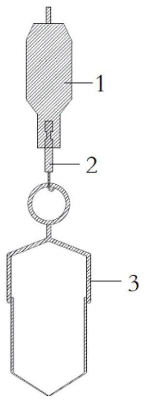
[0042] Taking a 6-inch [100] oriented single crystal with a 16-inch thermal field as an example, select the original doping device (structure such as figure 1 shown) and the doping device of the present invention (such as Figure 6 shown) doping the single crystal. (1) Statistics of different doping devices and the time required for the doping process; (2) Statistics of the resistivity of the single crystal head under the same doping amount and DBT time (5 hours) using different doping devices.

[0043] The specific doping method and related parameters of the original doping device are as follows:

[0044] (1) The molten polysilicon is stable at a certain temperature for 2 hours at a pressure of 20 Torr and a gas flow rate of 60 slpm;

[0045] (2) Close the isolation valve to separate the upper and lower furnace chambers, and the upper furnace chamber is inflated to 720 Torr to open;

[0046] (3) The seed crystal is removed, a doping device is installed, and the furnace doo...


PUM

PropertyMeasurementUnit
heightaaaaaaaaaa
diameteraaaaaaaaaa

Abstract

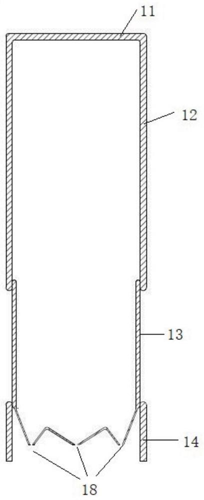
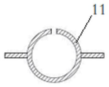
The invention discloses a doping device and a doping method for heavyly-antimony-doped Czochralski silicon. The doping device is made of transparent quartz glass and comprises a fixed bracket, a quartz cup for containing antimony and a bottom support, the fixed bracket comprises a fixed ring and a connecting rod, the fixed ring is circular, a notch is formed in the fixed ring, and the fixed ring is inserted and fixed above a seed crystal chuck through the notch; the upper part of the quartz cup is cylindrical, and the lower part of the quartz cup is funnel-shaped and consists of five small funnels; the upper end of the quartz cup is open, and the lower end is provided with a through hole at the bottom of each small funnel; and the bottom support is composed of four cylindrical quartz rods, and the quartz rods are symmetrically connected to the outer wall of the quartz cup. In the doping process, the doping device disclosed by the invention has the advantages that the doping device can be directly fixed above the seed crystal chuck, a seed crystal and a connector do not need to be disassembled and assembled, and five through holes are formed in the lower part of the quartz cup, so that the doping time is shortened; and the distance between the lower ends of the quartz rods of the bottom support and the lower end of the quartz cup is fixed, so the doping stability is improved.

Description

technical field [0001] The invention relates to a doping device and a doping method for heavily doped antimony Czochralski single crystal silicon, belonging to the technical field of Czochralski single crystal silicon. Background technique [0002] At present, semiconductor silicon materials can be divided into heavily doped silicon single crystals and lightly doped silicon single crystals. The resistivity value of a single crystal is determined by the doping amount of the selected doping element, the greater the doping amount of the doping element, the lower the resistivity of the single crystal. A single crystal with a large amount of doping is called a heavily doped silicon single crystal; conversely, a single crystal with a small amount of doping elements is called a lightly doped silicon single crystal. [0003] Among them, heavily doped silicon single crystal is the most ideal epitaxial substrate material, and its market demand continues to increase. Heavily doped si...

Claims


Application Information

Patent Timeline
Patent Type & Authority Applications(China)
IPC IPC(8): C30B15/04C30B29/06
CPCC30B15/04C30B29/06Y02P70/50
Inventor 王万华李超郑沉崔彬李英涛方峰
Owner GRINM SEMICONDUCTOR MATERIALS CO LTD
Learn More