Preparation method of voltage stabilizing diode with stable breakdown voltage

A voltage-stabilizing diode and breakdown voltage technology, which is applied in the field of diodes, can solve problems such as large changes in impurity concentration distribution and impact on breakdown voltage, and achieve reduced breakdown voltage changes, improved breakdown voltage stability, and good process compatibility sexual effect

Active Publication Date: 2021-06-15
XIAN MICROELECTRONICS TECH INST
View PDF9 Cites 0 Cited by
  • Summary
  • Abstract
  • Description
  • Claims
  • Application Information

AI Technical Summary

Problems solved by technology

[0004] The purpose of the present invention is to overcome the shortcomings of the above-mentioned prior art, and provide a method for improving the stability of the breakdown voltage of the Zener diode in the integrated circuit, so as to solve the problem of large changes in the impurity concentration distribution of the P-type region of the Zener diode in the prior art. Problems affecting breakdown voltage

Method used


Image

  • Preparation method of voltage stabilizing diode with stable breakdown voltage
  • Preparation method of voltage stabilizing diode with stable breakdown voltage
  • Preparation method of voltage stabilizing diode with stable breakdown voltage

Examples


Embodiment example 1

[0049] The Zener diode structure formed by the process method of the present invention is as follows:

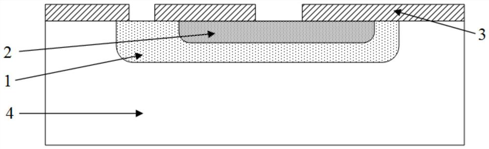
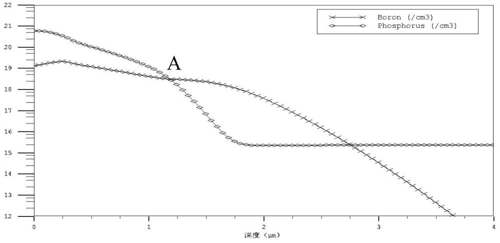
[0050] 1. The junction depth of the P-type region 1 of the Zener diode is 2.7 μm, and the doping concentration is 1.0E19cm -3 , the junction depth of the high-concentration N-type region 2 is 1.0 μm; the doping concentration is 1.0E20cm -3 ;

[0051] 2. Under the same breakdown voltage condition of the Zener diode, the standard deviation of the breakdown voltage of the Zener diode formed by the process method of the present invention is 0.02376, the standard deviation of the breakdown voltage of the traditionally formed Zener diode is 0.04967, and the voltage stabilizer formed by the new process method Diode breakdown voltage stability is higher than traditional technology.

[0052] This structure can be realized by the following methods:

[0053] 1. At a temperature of 950°C, a 100nm silicon dioxide layer 3 is grown on the silicon surface of the N-type substrate through ...

Embodiment example 2

[0061] The Zener diode structure formed by the process method of the present invention is as follows:

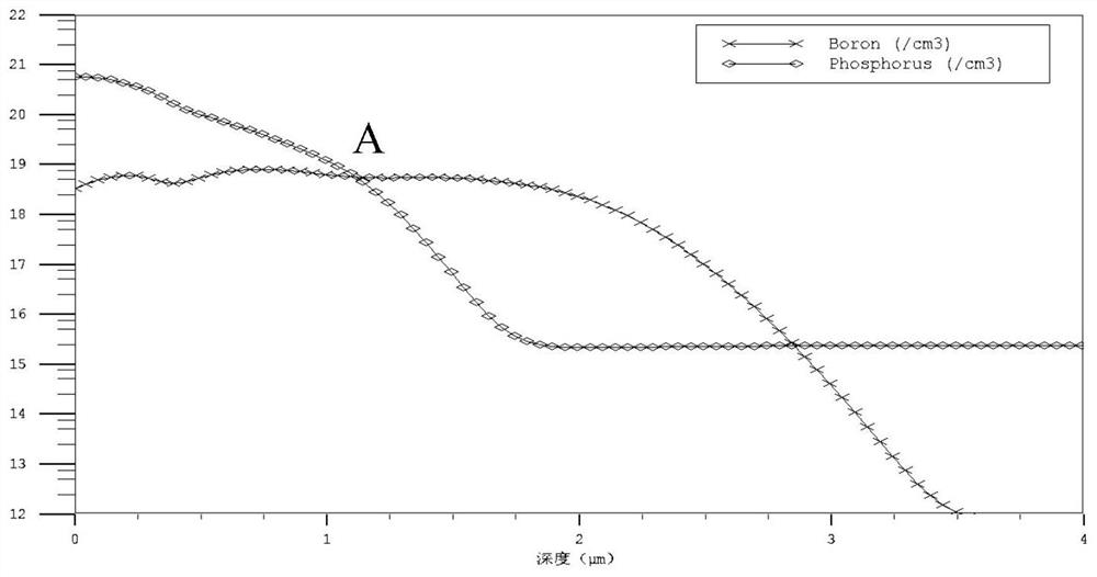
[0062] 1. The junction depth of the P-type region 1 of the Zener diode is 2.0 μm, and the doping concentration is 1.0E18cm -3 , the junction depth of the high-concentration N-type region 2 is 1.2 μm; the doping concentration is 1.0E20cm -3 ;

[0063] 2. Under the same breakdown voltage condition of the Zener diode, the standard deviation of the breakdown voltage of the Zener diode formed by the process method of the present invention is 0.03671, the standard deviation of the breakdown voltage of the traditionally formed Zener diode is 0.06053, and the voltage stabilizer formed by the new process method is 0.03671. Diode breakdown voltage stability is higher than traditional technology.

[0064] This structure can be realized by the following methods:

[0065] 1. At a temperature of 950°C, a 100nm silicon dioxide layer 3 is grown on the silicon surface of the N-type substr...


PUM

PropertyMeasurementUnit
thicknessaaaaaaaaaa
thicknessaaaaaaaaaa

Abstract

The invention discloses a preparation method of a voltage stabilizing diode with stable breakdown voltage, which is a process method for improving the stability of the breakdown voltage of the voltage stabilizing diode by adjusting the longitudinal distribution of impurities in a P-type region. By means of a high-energy ion implantation process , the impurity concentration gradient in the P-type region of the voltage stabilizing diode is reduced. Impurity activation of the P-type region of the voltage stabilizing diode is completed by adopting a low-temperature annealing or rapid annealing process after high-energy ion implantation, impurity concentration redistribution caused by a high-temperature thermal process is avoided, and the variation of the impurity concentration of the P-type region of the voltage stabilizing diode near a PN junction is reduced.

Description

【Technical field】 [0001] The invention belongs to the technical field of diodes, and in particular relates to a preparation method of a Zener diode with a stable breakdown voltage. 【Background technique】 [0002] The Zener diode refers to a diode that uses the reverse breakdown state of the PN junction to stabilize the voltage. Ensuring the stability of the reverse breakdown voltage of the Zener diode is the main parameter to characterize the process control capability of the Zener diode. [0003] see figure 1 , is a traditional zener diode structure. The zener diode is composed of a PN structure formed by a P-type region and a high-concentration N-type region. Its reverse breakdown voltage is determined by the base region / concentrated boron impurity concentration at the PN junction. In the traditional bipolar integrated circuit process, the P-type region of the Zener diode is formed at the same time as the base region of the NPN transistor, and the high-concentration N-ty...

Claims


Application Information

Patent Timeline
Patent Type & Authority Applications(China)
IPC IPC(8): H01L21/265H01L21/329H01L21/266H01L21/324H01L29/06
CPCH01L29/66128H01L29/66136H01L29/0684H01L21/266H01L21/26513H01L21/324Y02P70/50
Inventor 王清波薛东风薛智民孙有民赵杰
Owner XIAN MICROELECTRONICS TECH INST
Why Eureka
Try Eureka