Semiconductor package structure and manufacturing method thereof

A technology of packaging structure and manufacturing method, which is applied in semiconductor/solid-state device manufacturing, semiconductor device, semiconductor/solid-state device components, etc., can solve the problem of the increase of the residual copper ratio of the substrate, the mismatch of the thermal expansion coefficient between the substrate and the chip, and the overall semiconductor packaging structure. Volume increase and other issues to achieve the effect of reducing volume and avoiding expansion and contraction

Active Publication Date: 2021-08-06
FOREHOPE ELECTRONICS NINGBO CO LTD
View PDF3 Cites 0 Cited by
  • Summary
  • Abstract
  • Description
  • Claims
  • Application Information

AI Technical Summary

Problems solved by technology

However, this heat dissipation method will inevitably lead to an increase in the residual copper ratio inside the substrate, which will lead to expansion and contraction problems caused by the mismatch of thermal expansion coefficients between the substrate and the chip; the second is to mount heat dissipation metal on the substrate, In order to achieve heat dissipation by conducting the heat at the bottom of the chip to the heat dissipation metal, but this heat dissipation method will lead to an increase in the overall volume of the semiconductor package structure

Method used


Image

  • Semiconductor package structure and manufacturing method thereof
  • Semiconductor package structure and manufacturing method thereof
  • Semiconductor package structure and manufacturing method thereof

Examples


no. 1 example

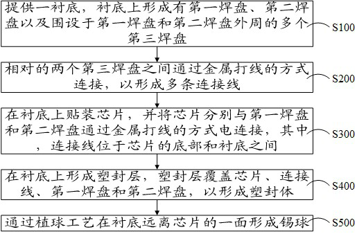
[0044] Please refer to figure 1 , the present embodiment provides a manufacturing method of a semiconductor package structure, the manufacturing method comprising:

[0045] S100 , providing a substrate on which a first pad 11 , a second pad 12 and a plurality of third pads 13 surrounding the first pad 11 and the second pad 12 are formed.

[0046] Wherein, both the first pad 11 and the second pad 12 are functional bonding pads of the chip 20 , and are used to realize the functional connection of the chip 20 . It should be understood that the first pad 11 and the second pad 12 should be electrically connected to corresponding functional pads on the chip 20 in one-to-one correspondence.

[0047] In addition, it should be noted that the number of the first bonding pads 11 and the second bonding pads 12 should be the same as the number of the corresponding functional bonding pads on the chip 20 , and there is a one-to-one correspondence.

[0048] The third pad 13 surrounds the ou...

no. 2 example

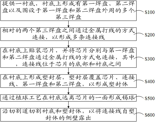
[0074] Compared with the first embodiment, the present embodiment differs in that, in the present embodiment, the above-mentioned plurality of third pads 13 are all provided on the dicing lines of the substrate (specifically, the substrate 10A).

[0075] In this way, please combine the reference image 3 , optionally, after forming the solder balls 40 on the side of the substrate away from the chip 20 through the ball planting process, the method further includes:

[0076] S600 , cutting the substrate and the molded package 30 along a dicing line, so as to expose the connecting wire 14 from the sidewall of the molded package 30 .

[0077] Such as Figure 7 As shown, after cutting the substrate and the plastic package 30 along the dicing line, the following can be obtained Figure 10 In the shown structure, at this time, a plurality of connecting wires 14 will be exposed from the side wall of the plastic package 30, thereby exposing the connecting wires 14 on the peripheral w...

no. 3 example

[0082] Compared with the first embodiment, this embodiment differs in that the lead frame 10B is used as the substrate in this embodiment (the substrate 10A is used as the substrate in the first embodiment).

[0083] In this embodiment, the substrate is a lead frame 10B, and a hollow area 15 is formed in the central area of ​​the lead frame 10B by etching, and a plurality of third bonding pads 13 are arranged around the hollow area 15 . Please refer to Figure 13 as shown, Figure 13 What is shown is a schematic structural view of the lead frame 10B.

[0084] It should be noted that the hollow area 15 is formed in the central area of ​​the lead frame 10B by etching, which may be by etching off the base island of the existing lead frame (the area produced after the base island is etched is the above-mentioned The hollowed-out area 15 ), thereby forming the lead frame 10B without base islands.

[0085] Please refer to Figure 11 Optionally, before the two opposite third pads...


PUM


Abstract

A semiconductor packaging structure and a manufacturing method thereof relate to the technical field of semiconductor packaging. The manufacturing method includes providing a substrate on which a first bonding pad, a second bonding pad, and a plurality of third bonding pads surrounding the periphery of the first bonding pad and the second bonding pad are formed; The three pads are connected by metal bonding to form multiple connection lines; the chip is mounted on the substrate, and the chip is electrically connected to the first pad and the second pad by metal bonding , wherein the connecting wire is located between the bottom of the chip and the substrate; a plastic encapsulation layer is formed on the substrate, and the plastic encapsulation layer covers the chip, the connecting wire, the first pad and the second pad to form a plastic package; through the ball planting process Solder balls are formed on the side of the substrate away from the chip. The manufacturing method of the semiconductor package structure can improve the heat dissipation effect of packaged products.

Description

technical field [0001] The invention relates to the technical field of semiconductor packaging, in particular to a semiconductor packaging structure and a manufacturing method thereof. Background technique [0002] With the rapid development of integrated circuits, the volume of the semiconductor packaging structure is getting smaller and smaller. At the same time, the power of the chips in the semiconductor packaging structure is increasing, which leads to the heat flux density in the semiconductor packaging structure (that is, the heat flux per unit area) The heat passing through the unit time in the section) is increasing day by day. As the heat flux density continues to increase, if the heat cannot be effectively dissipated, it is easy to cause the chip or system to be unable to use normally due to excessive temperature. [0003] In the traditional packaging process, the following two methods are usually used to dissipate heat. The first is to design a copper layer on t...

Claims


Application Information

Patent Timeline
Patent Type & Authority Patents(China)
IPC IPC(8): H01L23/31H01L23/495H01L21/56
CPCH01L23/3128H01L23/49568H01L21/56H01L2224/83385H01L2224/48227H01L2224/32225H01L2224/8592H01L2224/48091H01L2224/73265H01L2924/181H01L2924/15311H01L2224/97H01L2924/00014H01L2924/00012H01L2924/00
Inventor 张吉钦何正鸿张超
Owner FOREHOPE ELECTRONICS NINGBO CO LTD
Why Eureka
Try Eureka