SMD magnetic component and manufacturing method thereof

A magnetic component and patch technology, which is applied in the manufacture of inductors/transformers/magnets, electrical components, inductors with magnetic cores, etc., can solve problems such as crossing of inductive and outgoing lines, poor high-frequency characteristics, and interference from peripheral devices. Achieve the effects of small DC resistance, high Q value characteristics, and improved reliability

Active Publication Date: 2022-06-03
墨尚电子科技(江苏)有限公司
View PDF11 Cites 0 Cited by
  • Summary
  • Abstract
  • Description
  • Claims
  • Application Information

AI Technical Summary

Problems solved by technology

Under the influence of the high frequency trend, the former often leads to poor high frequency characteristics or even poor high frequency characteristics due to the crossover of winding wires and forming under pressure; RF inductors need to be able to control the inductance more accurately and obtain better Q value
[0003] The existing power inductor technology adopts the structure of one-piece molding or winding through convex buttons, such as the technologies disclosed in patents CN101553891B, US2016 / 0141087A1, CN110098042A, and CN104332275A. In the case of using a flat coil, there will still be crossing of the inductance and outgoing wires, which will affect reliability when used at high frequencies after pressure molding; another defect of this technology is that when the size becomes very flat, in order to obtain a higher Saturation current capability, the coil winding is very close to the outer wall of the component, a large amount of magnetic flux of the magnetic component will pass through the surrounding space, causing interference to the surrounding devices
[0004] In order to obtain a larger winding space in the existing RF wire-wound chip inductor or common mode inductor technology, U-shaped magnetic cores are usually used for winding and the terminals are directly formed on the ends of the U-shaped magnetic cores, such as patents CN201310351910.X, CN201410580127 .5, CN200910039475.0 and other disclosed technologies, the manufacturing process is simple, but there is a demand for more accurate control of the inductance, as well as greater current and better Q value

Method used


Image

  • SMD magnetic component and manufacturing method thereof
  • SMD magnetic component and manufacturing method thereof
  • SMD magnetic component and manufacturing method thereof

Examples


Embodiment 1

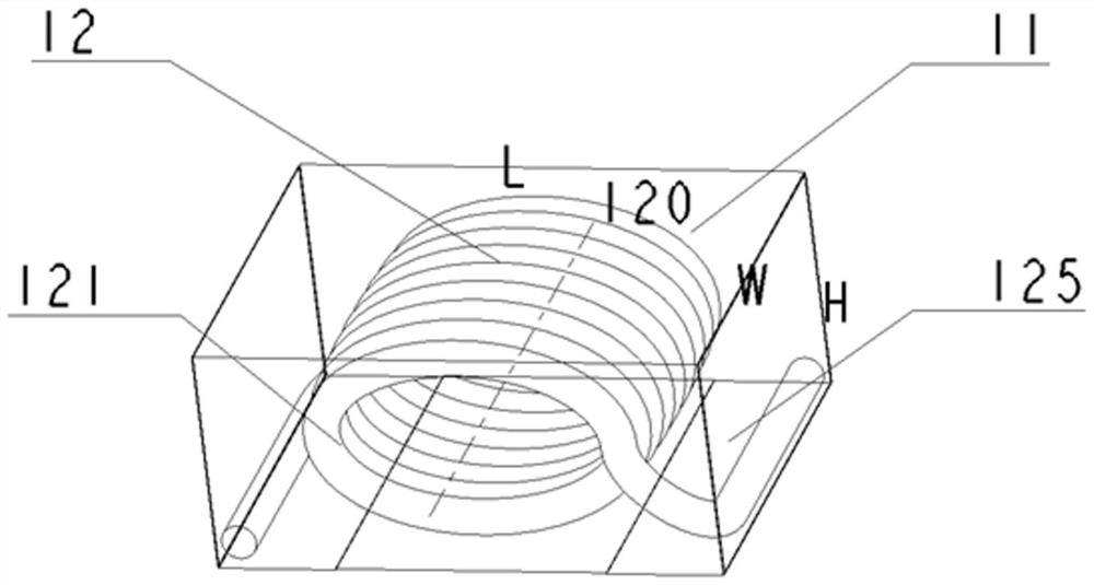
[0064] The perspective view of the structure of this embodiment is as follows figure 1 As shown, a chip magnetic element, whose length L≥width W≥height H, comprises: a coil winding 12, the winding axis 120 of which is parallel to the width W direction of the magnetic element, and the winding has both ends connected to plated terminals 125; The body 11 is included around the coil winding 12; the plated terminals 125 are distributed along the length L direction on the left and right sides of the winding axis 120, and in this embodiment, the plated terminals 125 are located on the bottom and side surfaces;

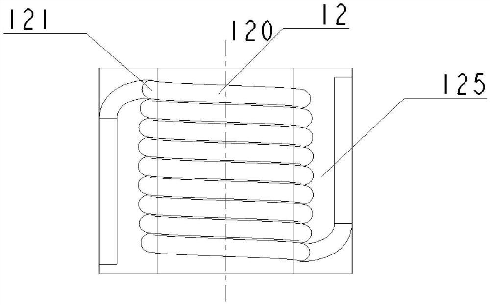
[0065] The outer shape of the coil winding 12 is elliptical, and the coil winding 12 has radian warped parts 121 in the length L direction on the left and right sides of the winding axis 120; figure 2 As shown, the coil winding 12 satisfies that its projection on the bottom LW plane at least partially falls within the plated terminal 125. It can be seen from the figure that ...

Embodiment 2

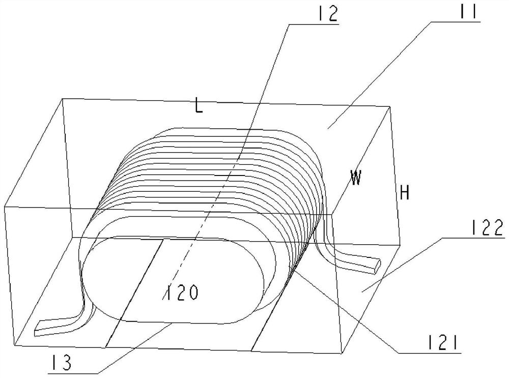
[0067] The perspective view of the structure of this embodiment is as follows image 3 As shown, a chip magnetic element, whose length L≥width W≥height H, comprises: a coil winding 12, the winding axis 120 of which is parallel to the width W direction of the magnetic element, and the winding has two ends connected to two copper The terminals 122 are connected by spot welding or thermocompression welding; the body 11 is included around the coil winding 12; the terminals 122 are distributed along the length L direction on the left and right sides of the winding axis 120. In this embodiment, the terminal electrodes 122 is on the bottom;

[0068] The shape of the coil winding 12 is a racetrack shape, and the coil winding 12 has radian warped parts 121 in the length L direction on the left and right sides of the winding axis 120; The magnetic element of this embodiment further includes a central column 13, which is made of iron-silicon-aluminum metal powder core; the coil winding ...

Embodiment 3

[0070] The appearance diagram of this embodiment is as follows Figure 4 As shown, a chip inductance element, the body 11 is electroplated with five-side electroplated terminals 125 . Its length L ≥ width W ≥ height H, such as Figure 5 As shown, it includes: a coil winding 12, the winding axis 120 of which is parallel to the width W direction of the magnetic element, and the winding has both ends connected to plated terminals 125; the body 11 is included around the coil winding 12; the The plated terminals 125 are distributed along the length L direction on the left and right sides of the winding axis 120 . In this embodiment, the plated terminals 125 are located on the upper and lower bottom surfaces and the side surfaces.

[0071] The shape of the coil winding 12 is a racetrack shape, and the coil winding 12 has radian warped parts 121 in the length L direction on the left and right sides of the winding axis 120; The magnetic element of this embodiment further includes a ...


PUM

PropertyMeasurementUnit
electrical resistanceaaaaaaaaaa
currentaaaaaaaaaa

Abstract

The invention provides a patch magnetic element and a manufacturing method thereof. The length L of the patch magnetic element ≥ width W ≥ height H; the patch magnetic element includes: a coil winding, and the winding axis of the coil winding is parallel to In the width W direction of the patch magnetic element, and having at least two ends; at least two terminals, connected to at least two ends of the coil winding and providing electrical contacts for connecting the patch magnetic element to a circuit; A body comprising a mixture of magnetic or non-magnetic material formed around at least a portion of the coil winding and exposing at least a portion of the terminals to mount the patch magnetics to the circuit. The stray capacitance of the winding wire of the present invention is very small, which reduces the influence of stray magnetic flux on peripheral components; the reliability is high; at the same time, the saturation current of the power inductor is larger than that of the prior art, and the DC resistance is smaller than that of the prior art.

Description

technical field [0001] The present invention relates to the field of electronic components, in particular, to a high-current thin chip magnetic component suitable for high-frequency applications and a manufacturing method thereof. Background technique [0002] There are mainly two types of winding solutions for the existing thin chip magnetic components, one is a traditional integrated inductor, and the other is to use an I-shaped magnetic core for winding, and the end of the magnetic core is electrically polarized to become a chip component. ; The former is often used as a power inductor, while the latter is used as a radio frequency inductor or a common mode inductor. Under the influence of the trend of high frequency, the former often has poor high-frequency characteristics or even bad because the windings are crossed and formed under pressure; RF inductors need to be able to control the inductance more accurately and obtain better Q value. [0003] The existing power i...

Claims


Application Information

Patent Timeline
Patent Type & Authority Patents(China)
IPC IPC(8): H01F27/28H01F27/30H01F27/29H01F27/36H01F27/02H01F41/063H01F41/066H01F41/00H01F17/04
CPCH01F27/2823H01F27/288H01F27/306H01F27/29H01F27/022H01F41/063H01F41/066H01F41/005H01F17/045H01F2017/046
Inventor 黄智褚江端悦涛
Owner 墨尚电子科技(江苏)有限公司
Why Eureka
Try Eureka